

Silylation treatment unit and method
a silylation treatment and treatment unit technology, applied in the direction of instruments, photomechanical equipment, photosensitive material processing, etc., to achieve the effect of preventing excessive silylation reaction, uniform density of silylation reagents, and reducing gas volum
- Summary
- Abstract
- Description
- Claims
- Application Information
AI Technical Summary
Benefits of technology
Problems solved by technology
Method used
Image

Examples
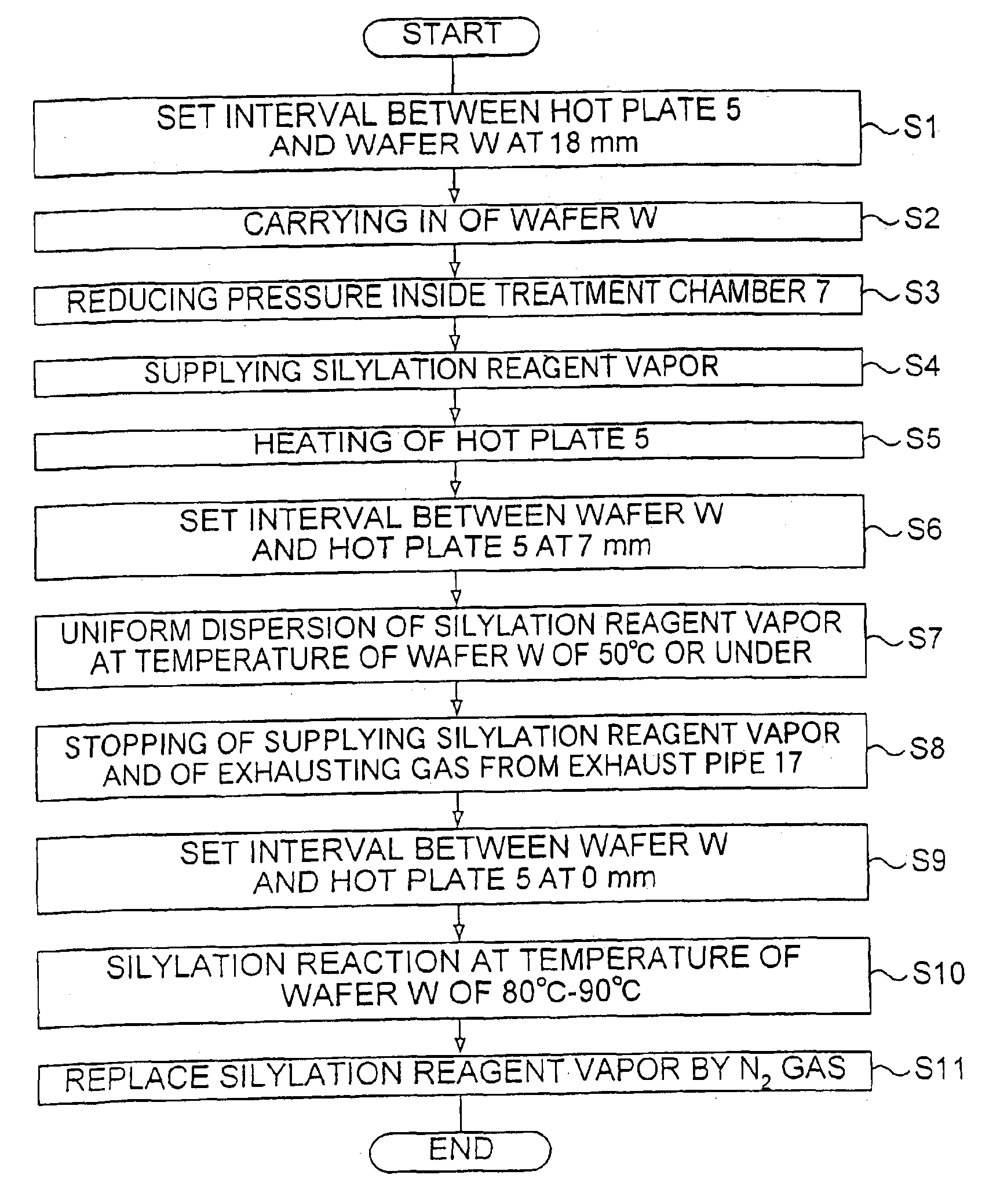
first embodiment
In this embodiment, a silylation treatment unit of the present invention which is applied to a resist treatment system for a semiconductor wafer will be explained.
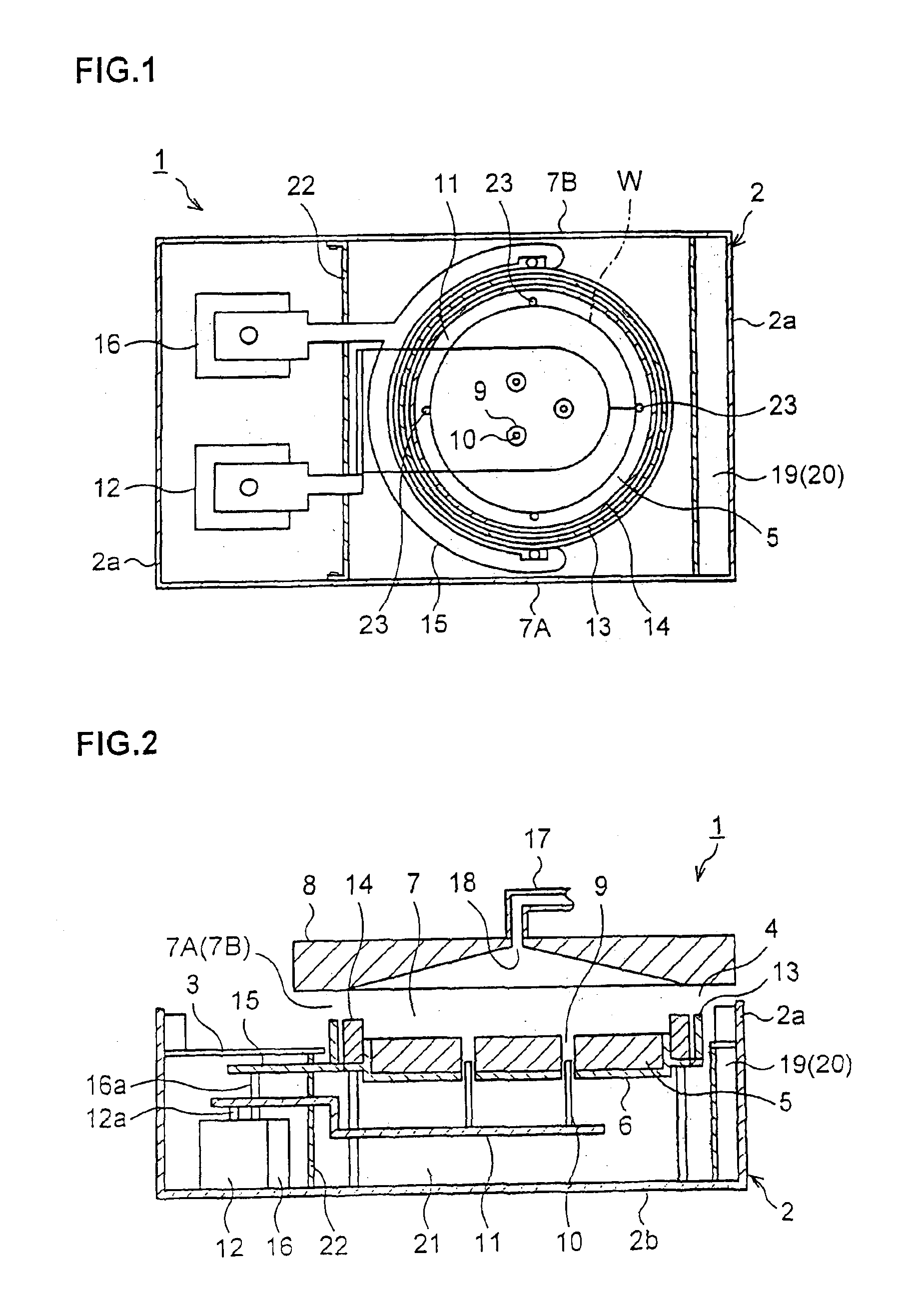
FIGS. 1 and 2 are a plane view and a vertical sectional view showing the structure of the silylation treatment unit, respectively.
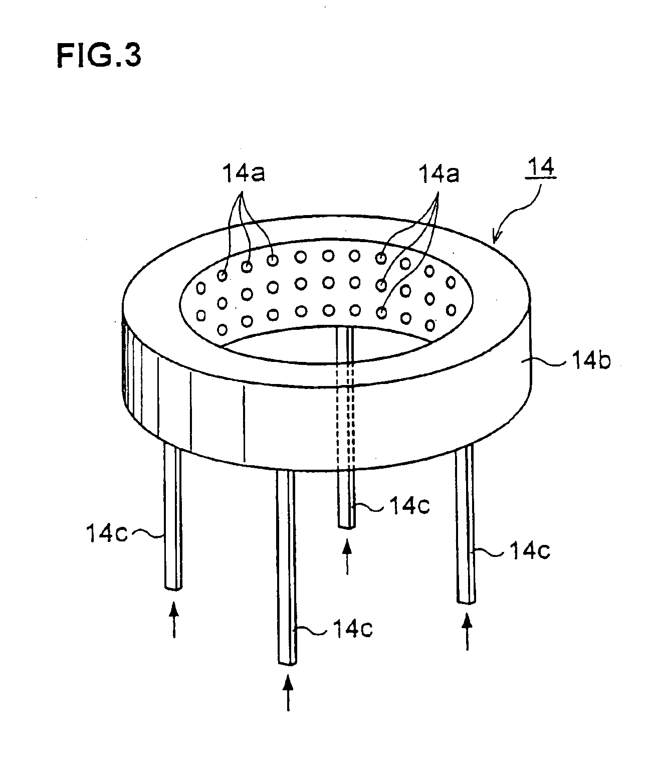
As shown in FIG. 1, a silylation treatment unit 1 includes a base block 2. The base block 2 is hollow and comprises a base block side portion 2a which defines its side and a base block bottom portion 2b which defines its bottom. Further, a horizontal masking shield 3 is attached horizontally to the base block bottom portion 2b at a position of a predetermined height of the base block side portion 2a. A circular opening 4 is formed in the horizontal masking shield 3 and a hot plate 5 is received as a heating mechanism in this opening 4. The horizontal masking shield 3 supports the hot plate 5 by a supporting plate 6.
A treatment chamber 7 for performing a silylation treatment is defined by the bas...
PUM
| Property | Measurement | Unit |
|---|---|---|
| central angle | aaaaa | aaaaa |
| pressure | aaaaa | aaaaa |
| temperature | aaaaa | aaaaa |
Abstract
Description
Claims
Application Information