Method for forming silicon film with changing grain size by thermal process

a technology of thermal process and silicon film, which is applied in the direction of bulk negative resistance effect devices, coatings, transistors, etc., can solve the problems of increasing the strength of electric fields across the tunnel dielectric, uneven upper surfaces of gates made in this manner, and uneven upper surfaces of gates, so as to minimize increase field strength. , the effect of increasing the strength of electric fields

Inactive Publication Date: 2005-03-29
MACRONIX INT CO LTD
View PDF25 Cites 4 Cited by
  • Summary
  • Abstract
  • Description
  • Claims
  • Application Information

AI Technical Summary

Benefits of technology

Floating gate elements with smooth lateral walls without “tips” can be fabricated by the deposition of “grainy” polysilicon. However, polysilicon floating gates made in this manner have an upper surface that is rough, rather than smooth as desired. Floating gates with smooth upper surfaces can be fabricated using amorphous silicon, but in this case, their lateral walls may have “tips” in the regions adjacent to the ONO tunnel oxide layer, which are undesirable because, being protrusions, their physical characteristics cause an increase in the strength of the electric fields across the tunnel dielectric. It is desirable to minimize the strength of the electric field between the floating gate and the substrate, because an increase in field strength causes a greater loss by leakage of the charge stored in the floating gate.
Accordingly, there is a need for techniques that improve the manufacture of transistor floating gates, wherein the floating gates exhibit the desired properties of smoother lateral walls with reduced “tips” adjacent to their ONO tunnel oxide layers, and which also have smoother upper surfaces adjacent to their control gate dielectric layer.
Roughly described, the seemingly contradictory objectives of reduced tip adjacent the tunnel dielectric layer and increased smoothness adjacent the gate dielectric layer can both be achieved by forming a silicon layer that transitions from polysilicon at one surface to amorphous silicon at the opposite surface. The transition can be monotonic, and can be either continuous or it can change abruptly from polysilicon to amorphous silicon. If such a layer is formed as the floating gate of a floating gate transistor structure, the larger grain structure adjacent to the tunnel dielectric layer can reduce the formation of a tip and thus reduces leakage. On the other hand, the smaller grain structure adjacent to the gate dielectric layer can produce a smoother, more uniform gate dielectric layer. The polysilicon-to-amorphous silicon transistor can be fabricated with a temperature profile that favors polysilicon formation at the start of floating gate deposition, and transitions during deposition to a temperature that favors amorphous silicon deposition at the end of floating gate deposition.

Problems solved by technology

This is true, because it is believed that such protrusions or tips, especially when located near the tunnel oxide layer, result in increased electric fields, and therefore, increased leakage of the charge stored on the floating gate, thus impairing the gate's ability to retain a stored data value over time.
However, polysilicon floating gates made in this manner have an upper surface that is rough, rather than smooth as desired.
Floating gates with smooth upper surfaces can be fabricated using amorphous silicon, but in this case, their lateral walls may have “tips” in the regions adjacent to the ONO tunnel oxide layer, which are undesirable because, being protrusions, their physical characteristics cause an increase in the strength of the electric fields across the tunnel dielectric.

Method used


Image

  • Method for forming silicon film with changing grain size by thermal process
  • Method for forming silicon film with changing grain size by thermal process
  • Method for forming silicon film with changing grain size by thermal process

Examples


Embodiment Construction

The following detailed description is made with reference to the figures. Certain embodiments are described to illustrate the present invention, not to limit its scope, which is defined by the claims. Those of ordinary skill in the art will recognize a variety of equivalent variations on the description that follows.

A semiconductor device may be fabricated by processes that include the formation of multi-layer assemblies through vapor deposition onto a substrate structure. In addition, the electrical properties of the multi-layer assemblies used to form device microstructures can be modified during deposition by the selective inclusion of other elements or compounds during or after the deposition process, to obtain results referred to as “doping.”

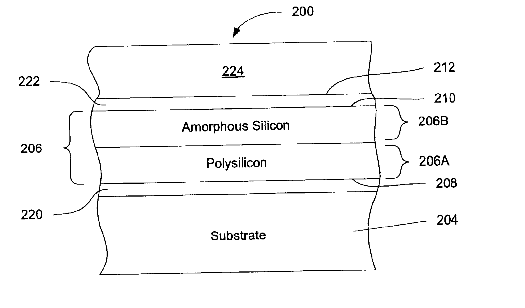
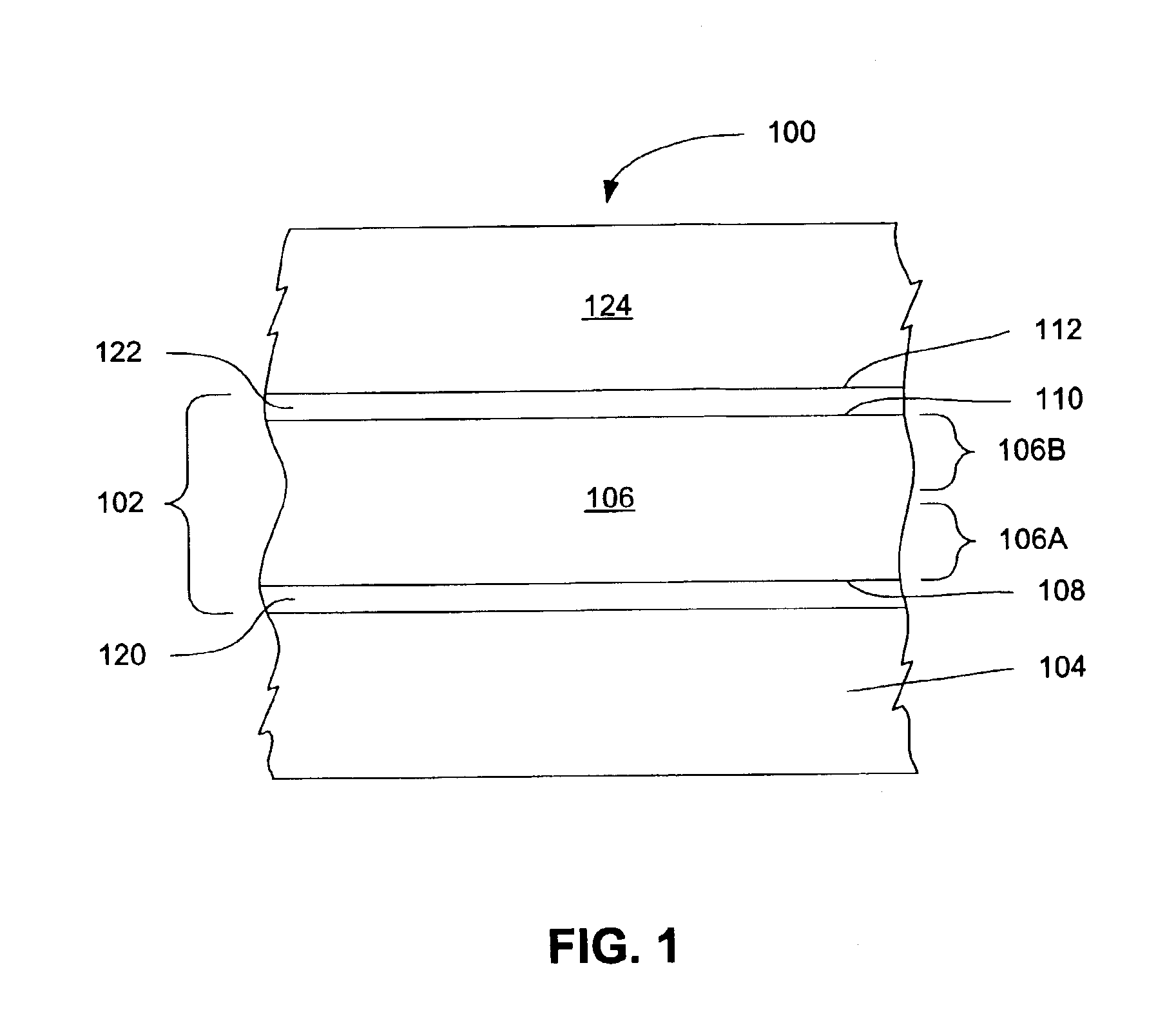
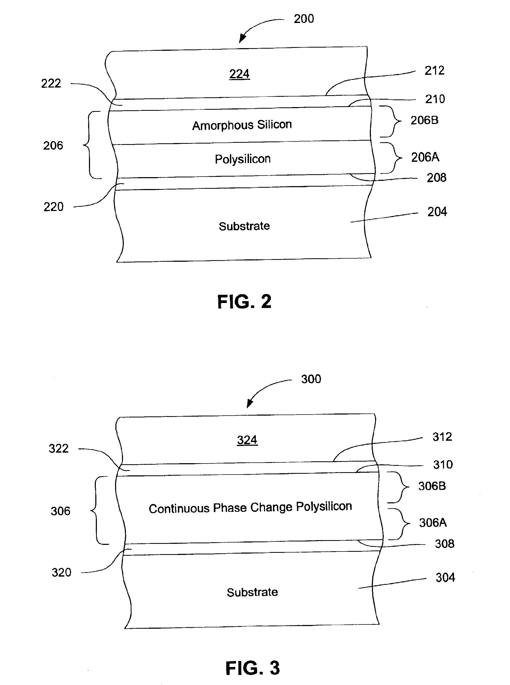
FIG. 1 is a cross-section diagram of a silicon device structure 100, incorporating features of the invention. The structure comprises a substrate 104, a multi-layer assembly 102 superposed on the substrate, and at least one additional layer...


PUM

PropertyMeasurementUnit
temperatureaaaaaaaaaa

Abstract

Roughly described, a silicon layer transitions from polysilicon at one surface to amorphous silicon at the opposite surface. The transition can be monotonic, and can be either continuous or it can change abruptly from polysilicon to amorphous silicon. If such a layer is formed as the floating gate of a floating gate transistor structure, the larger grain structure adjacent to the tunnel dielectric layer reduces the formation of a tip (protrusion) and thus reduces leakage. On the other hand, the smaller grain structure adjacent to the gate dielectric layer produces a smooth, more uniform gate dielectric layer. The polysilicon-to-amorphous silicon transistor can be fabricated with a temperature profile that favors polysilicon formation at the start of floating gate deposition, and transitions during deposition to a temperature that favors amorphous silicon deposition at the end of floating gate deposition.

Description

BACKGROUND OF THE INVENTIONThe present invention relates to the field of semiconductor device fabrication, and to the formation within such devices of silicon microstructures through the use of chemical vapor deposition, dopant implantation, feature patterning and etching, and other fabrication techniques. Furthermore, polysilicon is a material widely used in microelectronic devices, and the present invention relates to certain fabrication methods and device structures that may require the use of polysilicon. More particularly, in certain memory devices, polysilicon may be employed for floating gates of transistors used to form a storage array. In memory device applications of this type, the transistor floating gates are used to store and retain a plurality of electrical charges in accordance with the data being written. Subsequent read operations may then be performed on a device to retrieve stored data when it is needed.In the manufacture of semiconductor devices, the structure of...

Claims


Application Information

Patent Timeline
Patent Type & Authority Patents(United States)
IPC IPC(8): H01L29/423H01L29/40H01L29/49H01L21/205
CPCH01L29/42324H01L29/4925H01L21/0262H01L21/02532H01L21/0245
Inventor HUANG, CHIH YUANCHEN, JONASON
Owner MACRONIX INT CO LTD
Why Eureka
Try Eureka