

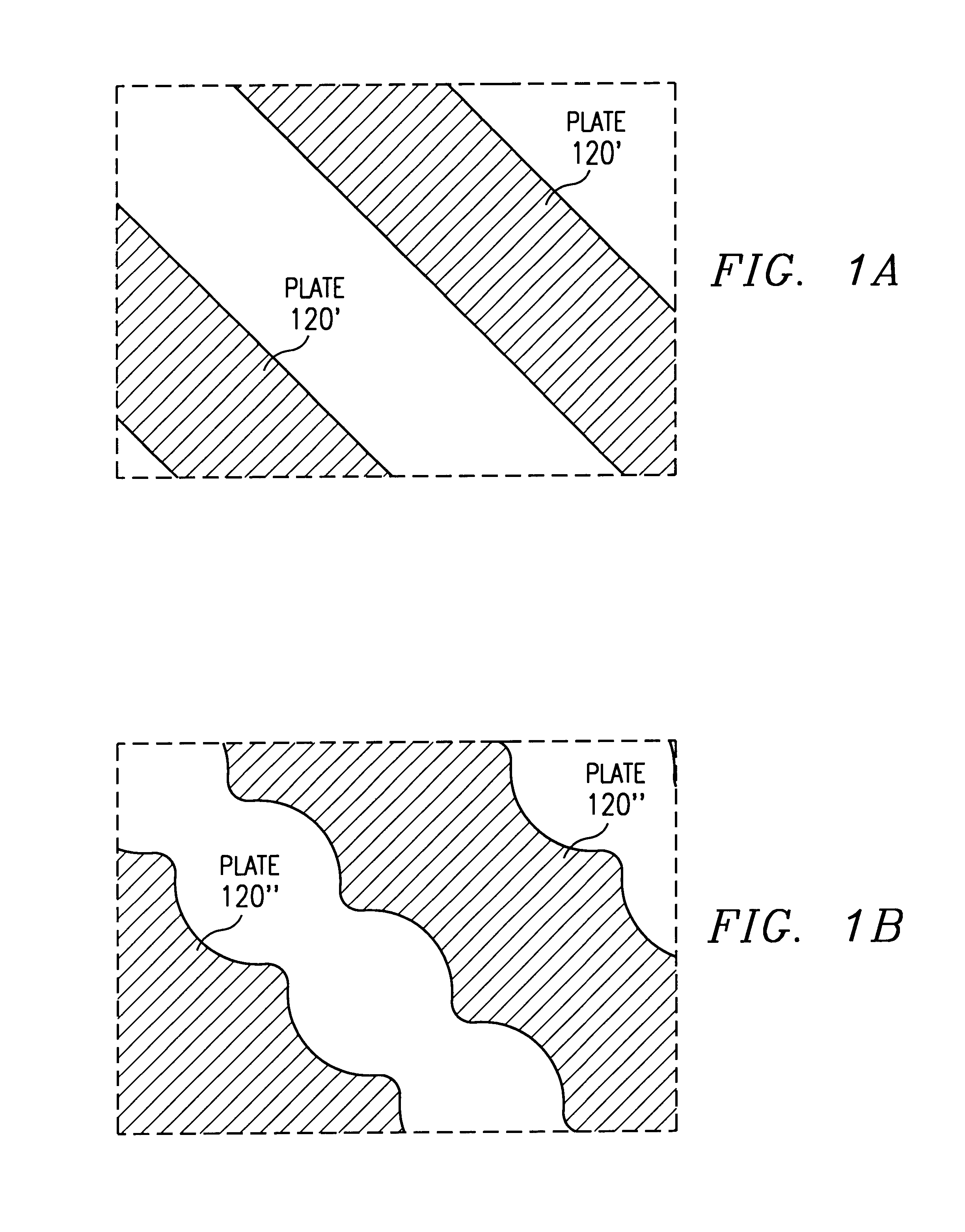
Reduced size plate layer improves misalignments for CUB DRAM
a technology of plate electrodes and misalignments, applied in the direction of capacitors, solid-state devices, transistors, etc., can solve the problems of large misalignment between layers, complex structure, and inability to meet the needs of dram cells, so as to reduce the size of the plate electrode, simplify the alignment, and reduce the contribution of the plate electrode to the total capacitance. field
- Summary
- Abstract
- Description
- Claims
- Application Information
AI Technical Summary
Benefits of technology
Problems solved by technology
Method used
Image

Examples
embodiment
Primary Embodiment
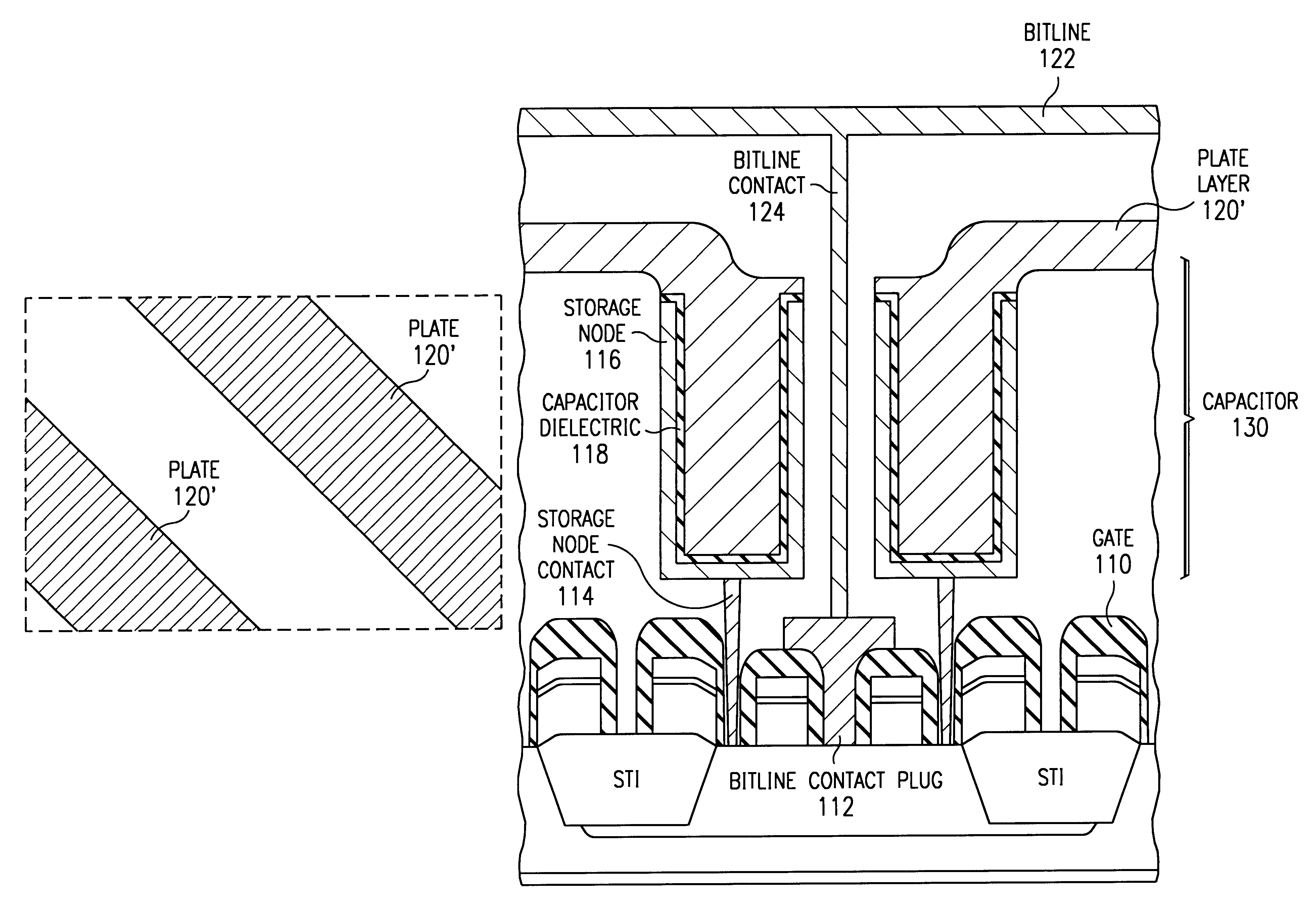
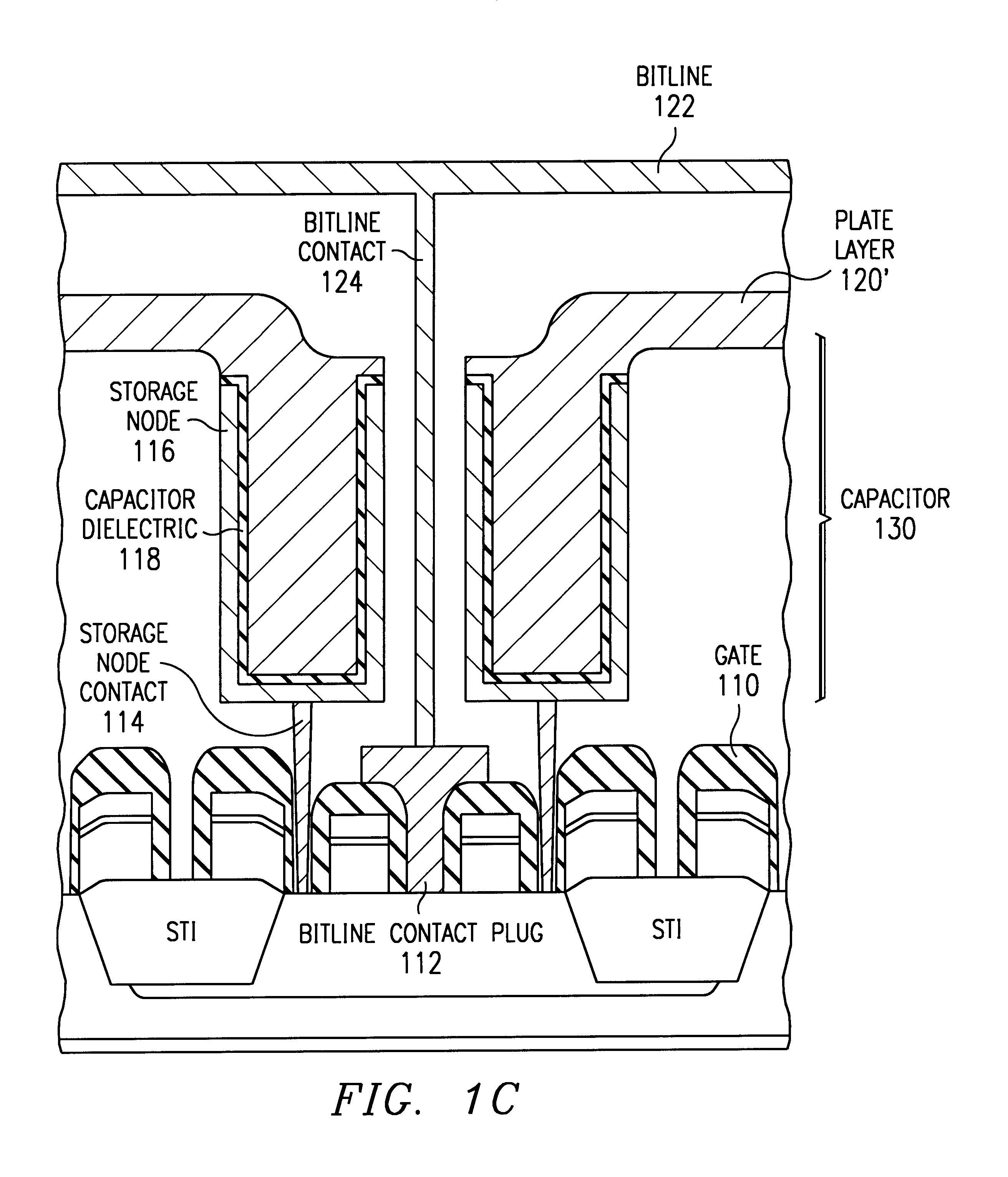
Formation of the disclosed CUB DRAM cells will now be discussed with reference to the flowchart of FIG. 9, which will be discussed in connection with FIGS. 2A-F and 3A-H, which show overviews and cross-sections respectively of the DRAM array during stages of processing.
Isolation structures are first formed on the wafer substrate, such as the shallow trench isolation shown in FIG. 3A, leaving the soon-to-be active areas 108 exposed. FIG. 2A shows an “overhead” view of the wafer, showing the pattern of active areas, with a grid pattern shown merely for convenience. Transistors are formed, including gate structures 110. The gate stack preferably (but not necessarily) comprises polysilicon, TiN, and tungsten. FIG. 3B and FIG. 2B show the array once the transistors are completed (step 110).
A layer of dielectric is deposited, e.g. 5 nm of SiO2. As seen in FIG. 3C and FIG. 2C, a contact is etched between selected gates, and filled with polysilicon to form a plug 112 to re...
PUM
 Abstract
Description
Claims
Application Information