

Semiconductor device having capacitors for reducing power source noise
a technology of capacitors and power sources, applied in the field of semiconductor devices, can solve the problems of generating electromagnetic waves from the semiconductor chip, and reducing the immunity of the chip to power source noise, so as to reduce the effect of power source noise reduction, reduce the inductance between the chip capacitors and the semiconductor chip, and reduce the effect of power source noise effective
- Summary
- Abstract
- Description
- Claims
- Application Information
AI Technical Summary
Benefits of technology
Problems solved by technology
Method used
Image

Examples
first embodiment
The first embodiment of the present invention will now be described with reference to FIG. 1.
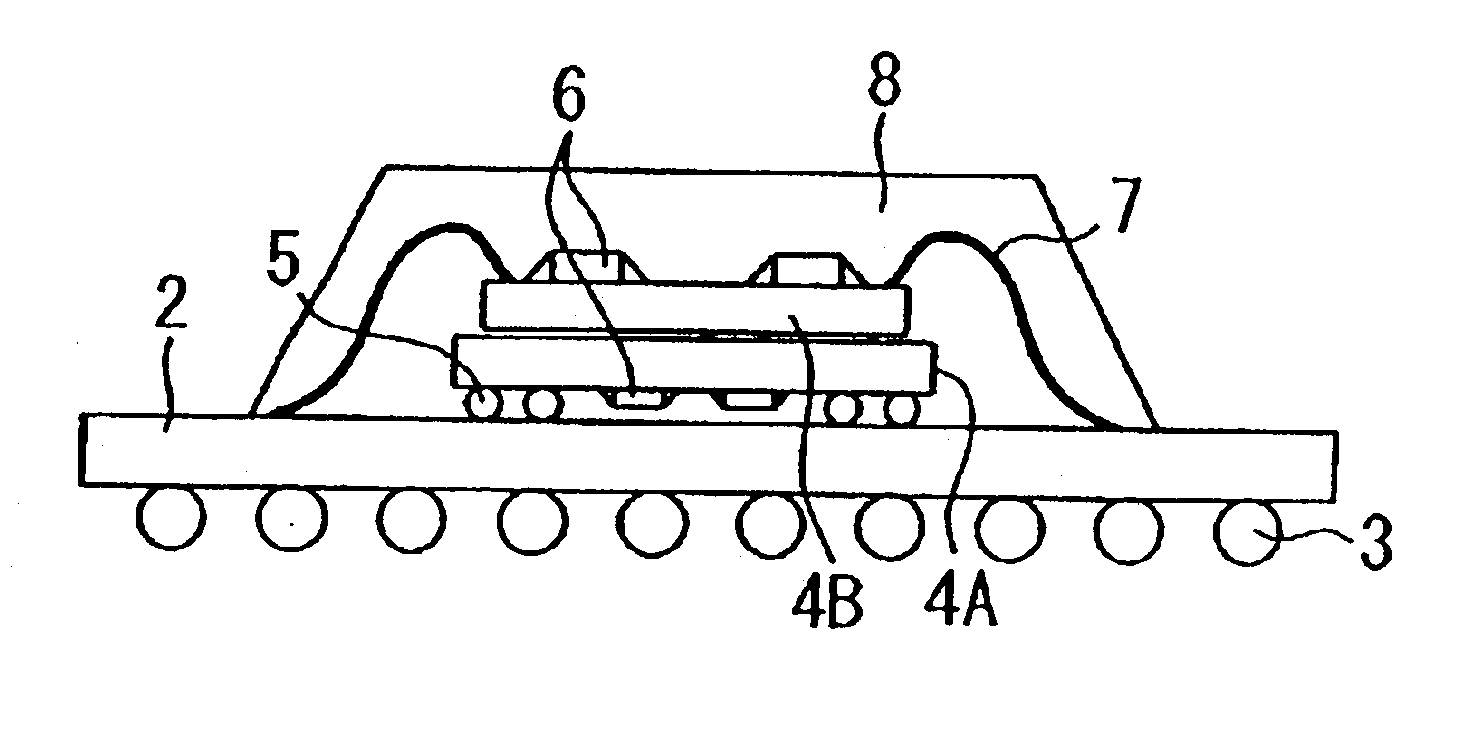
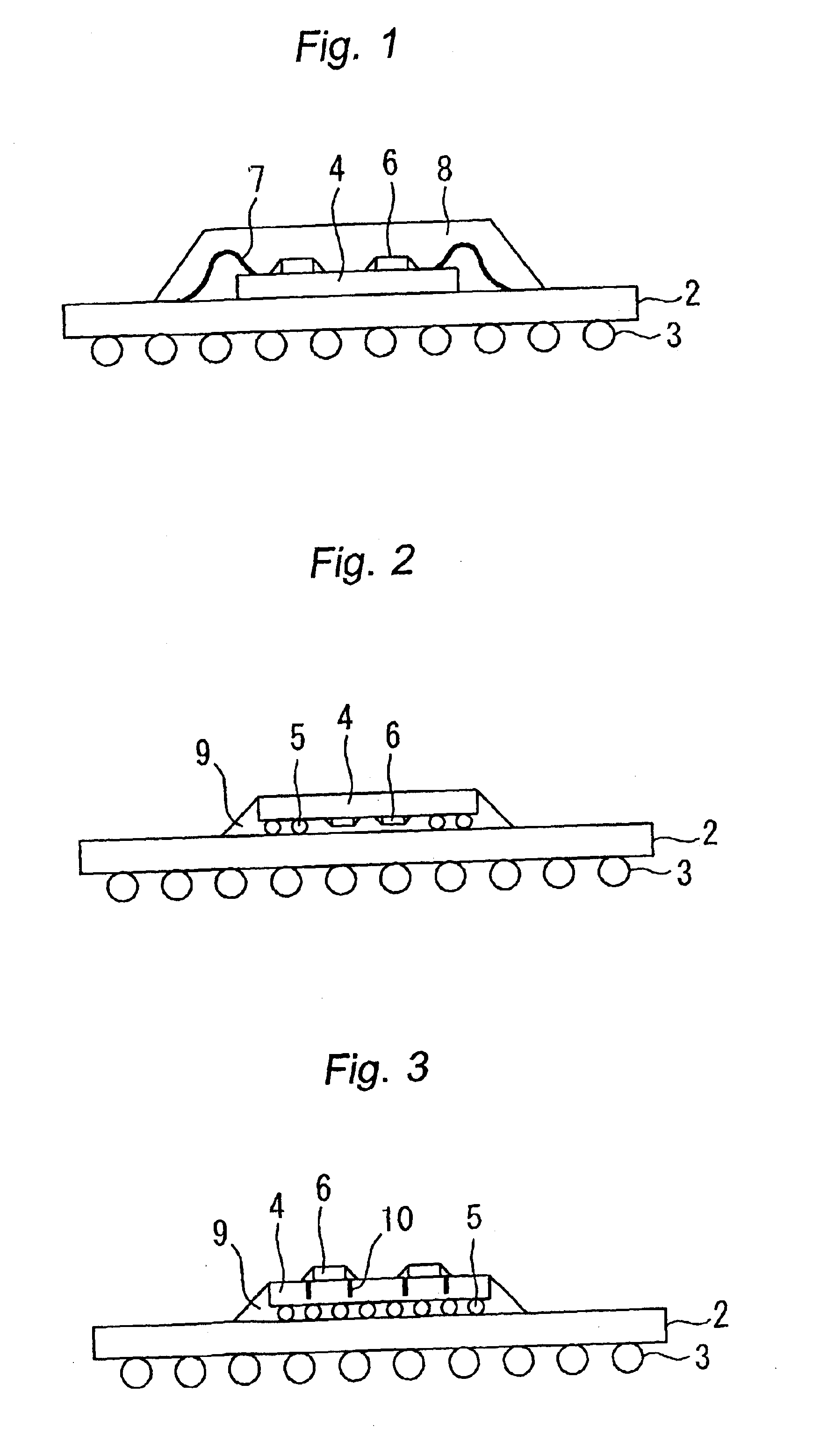
FIG. 1 is a cross-sectional view for describing a typical structure of a semiconductor device according to a first embodiment of the present invention. In FIG. 1, reference numeral 2 indicates a BGA (ball grid array) substrate. The BGA substrate 2 is secured onto a mounting substrate (not shown), with numerous solder balls 3 interposed therebetween to ensure inter-substrate electrical connection in a well-known procedure.
Reference numeral 4 indicates a semiconductor chip mounted on the BGA substrate 2. Metal wires 7 provide electrical connection between the semiconductor chip 4 and the BGA substrate 2. Reference numeral 6 indicates chip capacitors provided for the same technical reason as in conventionally devised comparable setups. What characterizes the first embodiment is that the chip capacitors 6 are mounted on the semiconductor chip 4. Reference numeral 8 indicates a mold resin that co...
second embodiment
The second embodiment of the present invention will now be described with reference to FIG. 2.
FIG. 2 is a cross-sectional view for describing a typical structure of a semiconductor device according to the second embodiment. In FIG. 2, the component parts having the same or corresponding functions as their counterparts in FIG. 1 are designated by like reference numerals, and their descriptions are omitted where redundant.
What makes the second embodiment different form the setup of FIG. 1 is that bumps 5 are used to connect the semiconductor chip 4 with the BGA substrate 2. In FIG. 2, reference numeral 5 indicates bumps that secures the semiconductor chip 4 onto the BGA substrate 2 while providing electrical connection therebetween.
Whereas the metal wires 7 in the first embodiment of FIG. 1 tend to constitute prolonged connections that may entail worsened electrical characteristics, the bumps 5 eliminate that potential problem.
Because the semiconductor chip 4 furnished with the bumps ...
third embodiment
The third embodiment of the present invention will now be described with reference to FIGS. 3 and 4.
FIG. 3 is a cross-sectional view for describing a typical structure of a semiconductor device according to the third embodiment. In FIG. 3, the component parts having the same or corresponding functions as their counterparts in FIG. 2 are designated by like reference numerals, and their descriptions are omitted where redundant.
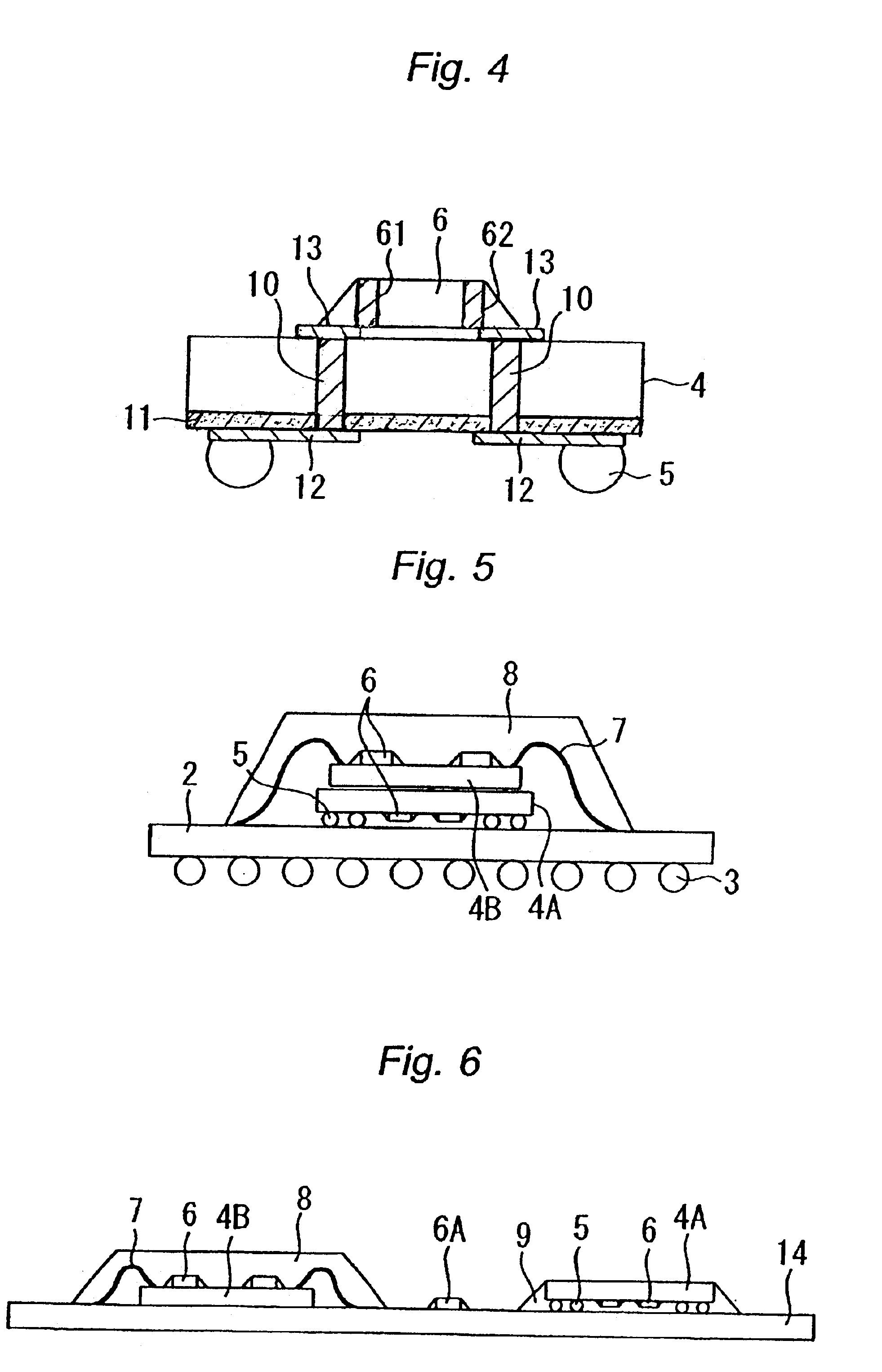
What differentiates the third embodiment from the setup of FIG. 2 is that while chip capacitors 6 are attached to the back of the semiconductor chip 4, a plurality of through-type via contacts 10 are used to ensure electrical connection between the chip capacitors 6 and active regions of the semiconductor chip 4. In FIG. 3, reference numeral 6 indicates chip capacitors 6. The chip capacitors 6 are mounted on the top, as shown in FIG. 3, which in fact constitutes the back of the semiconductor chip 4.
Reference numeral 10 indicates through-type via contact that ext...
PUM
 Abstract
Description
Claims
Application Information