Electronic switch

a technology of electronic switch and switch, applied in the field of electronic switch, can solve the problems of increasing the pinch-off voltage of the fets, narrow limits are imposed by the limited voltage sustaining capability of metal-semiconductor junction, and the effect of increasing the switching time of the electronic switch

Inactive Publication Date: 2005-03-29
ROHDE & SCHWARZ GMBH & CO KG
View PDF3 Cites 22 Cited by
  • Summary
  • Abstract
  • Description
  • Claims
  • Application Information

AI Technical Summary

Benefits of technology

Because of the implementation of the conversion device with a high input impedance and a low output impedance, it becomes possible to allow the input signal to be coupled out without reactive effects.
If the switching apparatus, which brings about the two switching states, is made with FET or n-MESFET on a basis of silicon or gallium arsenide on a semiconductor chip, then it is possible that the electronic switch, with its switch apparatus, can be constructed with especial simplicity. Added to this advantage, is the fact that especially low switching times, i.e., reaction times, are achieved and the switch apparatus can be integrated together with other components of the electronic switch on a semiconductor chip.
In this manner, then both in the ON-state as well as in the OFF-state, an improvement of the low frequency large signal behavior of the electronic switch is achieved. Especially advantageous is again the choice of holding the first DC potential at a lower level, i.e., more negative, than the pinch-off voltage of the field effect switch transistor, and the second voltage is made as high as the reference potential. In this way, in an advantageous manner, the ON-state is made by adding the second DC voltage and the OFF-state is achieved by adding the first DC voltage to the correction signal, which is continuously connected to the control port.

Problems solved by technology

The disadvantage found in the electronic switch as taught by U.S. Pat. No. 5,107,152 lies therein, in that because of the diodes, the switching time of the electronic switch is essentially increased.
Finally, the pinch-off voltage of the FETs can be increased by modification of the manufacture process, whereby, especially in the case of MESFETs, narrow limits are imposed by the limited voltage sustaining capability of metal-semiconductor junctions when operated in reverse direction.

Method used


Image

  • Electronic switch
  • Electronic switch
  • Electronic switch

Examples


Embodiment Construction

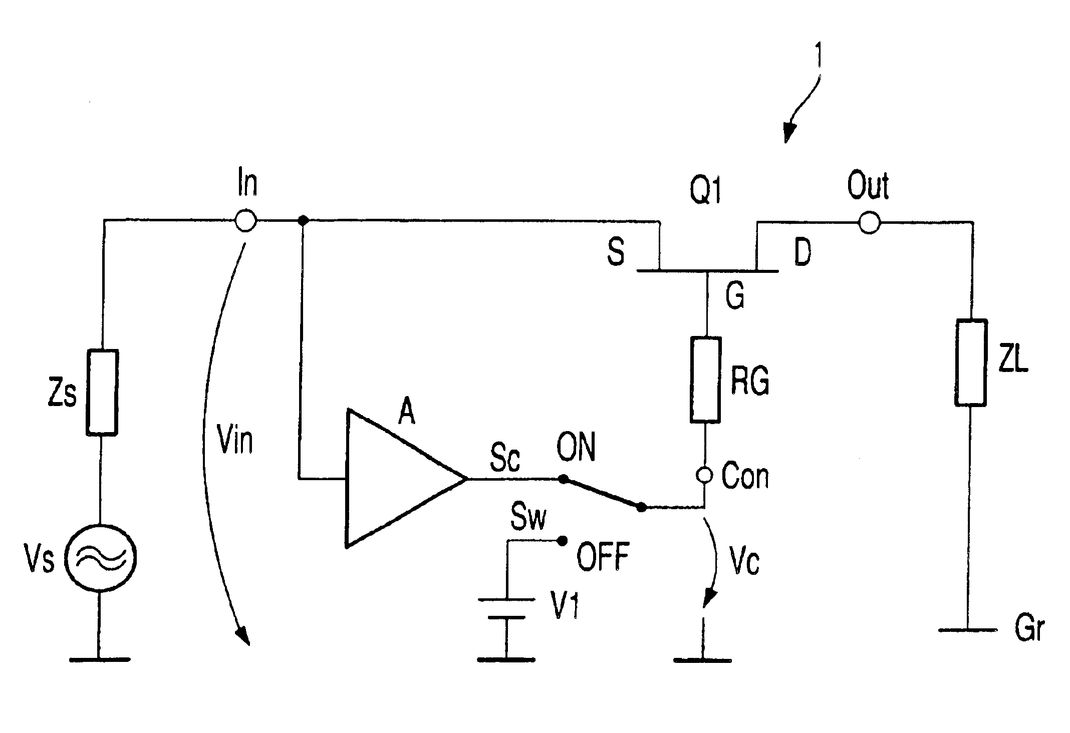
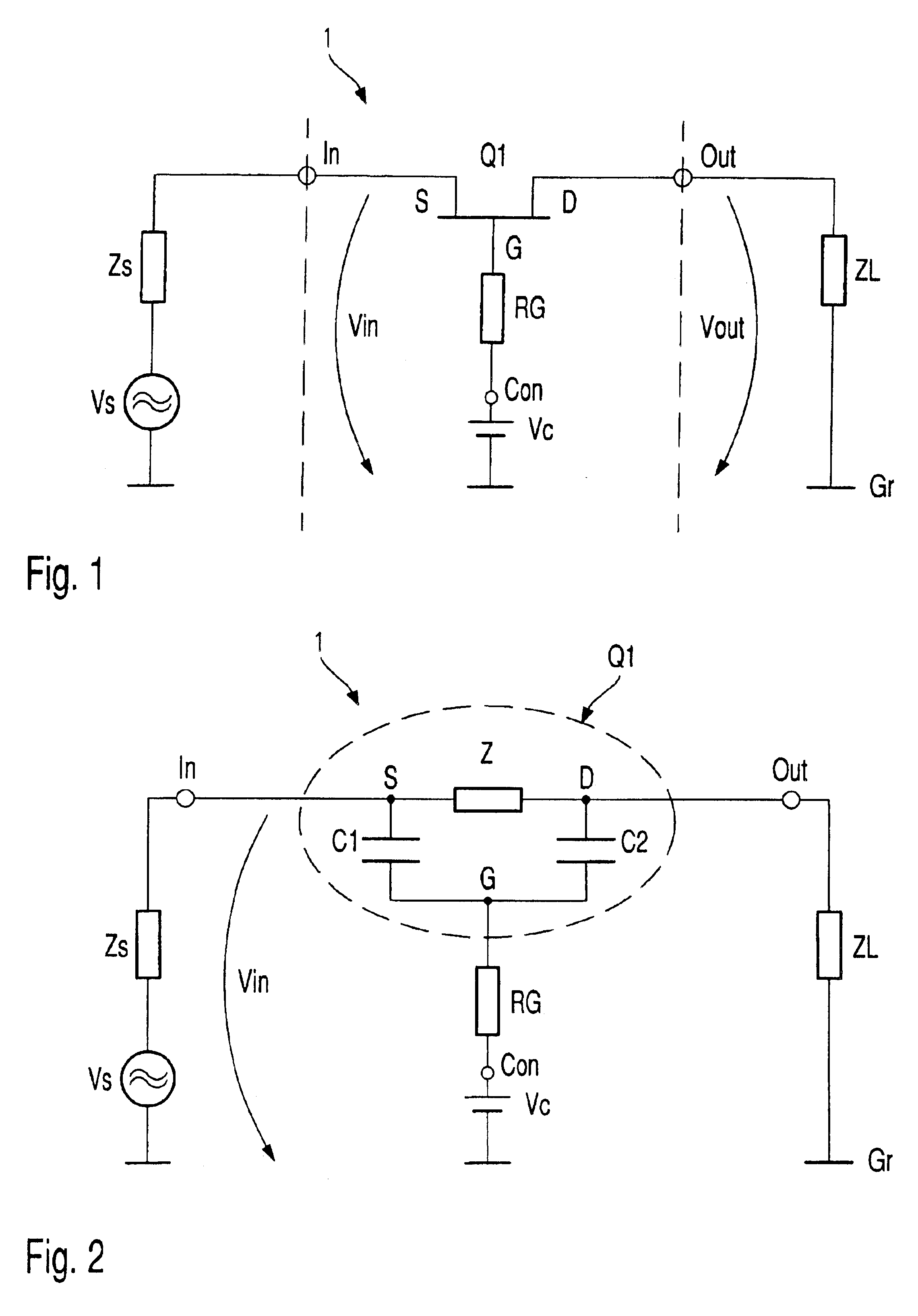
FIG. 1 shows an electronic switch 1 with an FET Q1 in accordance with the state of the technology. The FET Q1 has a gate terminal G connected to a control port Con through a first resistance RG. Also depicted is a source terminal S connected to an input In and a drain terminal D connected to an output Out. A control signal Vc applied to the control port Con, whose value in this embodiment can assume two different DC voltages, controls the switching state of the electronic switch 1.

The value of the DC voltage is, for example, altered by a switching apparatus not shown in FIG. 1. Usually one of the two DC values is equal to 0 V, with reference to a common reference potential Gr. With self conducting, n-channel metal semiconductor field-effect transistors, preferred in microwave technology, this value of DC voltage establishes the ON-state. In the ON-state, the FET Q1 switches an input signal Vin, which is present at the input port In directly through to the output port Out. The input ...


PUM


Abstract

Electronic switch (1) with two switching states (ON, OFF) possesses at least one field effect switching transistor (Q1), input port (In) connected with source terminal (S), on which input signal (Vin) is present, output port (Out) connected with drain terminal, on which switched signal (Vout) is present, control port (Con) connected to gate terminal (G), on which is present signal (Vc) for controlling electronic switch (1) and switch apparatus (Sw), which creates the two switching states (ON, OFF) by means of a changing of control signal (Vc). Controlling signal (Vc), during at least one of the two switching states (ON, OFF) is, at least partially, formed by correction signal (Sc), which in turn is produced from input signal (Vin), so that the frequency dependent drop in voltage between the drain-source channel and the gate electrode of the field effect switching transistor (Q1) is at least partially compensated.

Description

BACKGROUND OF THE INVENTIONThe invention concerns an electronic switch with a field effect transistor (FET). The electronic switch serves for rapid switching of broadband, high frequency signals of high amplitude dynamics.Electronic switches, for example, are employed in high frequency technology in signal attenuators with switchable attenuation stages. To this purpose, mostly FETs are used, connected in series, or for very high frequency and broadband applications, metal, semiconductor field effect transistors (MESFET) are employed. The bandwidths run, for example, from 1 GHz up to several multiples of 10 GHz. Usually, n-channel-MESFET on a gallium arsenide basis is chosen.Such an electronic switch, for example, is made known by U.S. Pat. No. 5,107,152. The circuit disclosed in that patent, with the aid of a diode connected in series with a control port, attempts to improve the low frequency, large signal behavior of the switch, which is governed essentially by the voltage drop ove...

Claims


Application Information

Patent Timeline
Patent Type & Authority Patents(United States)
IPC IPC(8): H03K17/16H03K17/06
CPCH03K17/162H03K17/063
Inventor EVERS, CHRISTIANCOHRS, WOLFGANGRICHTER, WOLFGANGWILL, THOMASHASSLER, MARTIN
Owner ROHDE & SCHWARZ GMBH & CO KG
Why Eureka
Try Eureka