Data processor memory circuit

a memory circuit and data processor technology, applied in the field of memory circuits, can solve the problems of increasing static power consumption, reducing the switching time, and losing any information stored in the memory cell when switched into low-leakage mode, so as to reduce the switching time, reduce the leakage through the pass transistor, and increase the threshold voltage

Active Publication Date: 2006-05-30
ARM LTD +1
View PDF4 Cites 49 Cited by
  • Summary
  • Abstract
  • Description
  • Claims
  • Application Information

AI Technical Summary

Benefits of technology

[0032]In a preferred embodiment, memory cell transistors of the memory's internal inverters are coupled to read / write lines of the memory circuit via a pass-transistor having a substantially higher threshold voltage than the associated cell transistors. This has the advantage of significantly reducing leakage through the pass transistors when the read / write lines are maintained in high-power mode.
[0033]In a further preferred embodiment, the memory circuit is arranged such that the capacitance of the voltage supply rail (which supplies voltage Vdd) is substantially less than the capacitance of pass-transistor. This has the advantage that it reduces the switching time for the transition between the readable state and the unreadable state, allowing for shorter switching times than achievable using techniques that involve increasing the threshold voltage of the memory cell transistors.
[0034]There are several alternative ways of allowing for cell information to be retained in the low-leakage mode. However, preferred embodiments achieve this objective by providing a memory circuit in which, in the unreadable state the first voltage (i.e. the supply voltage Vdd) is to set to be substantially 1.5 times the threshold voltage associated with the memory cell transistors. This provides for straightforward implementation of memory retention in the unreadable state.
[0035]Advantageously, in preferred embodiments transitions between the readable state and the unreadable state are effected by changing the supply voltage from a high value in the readable state to a comparatively low value in the unreadable state. This has the advantage that the change to the supply voltage in switching from the readable state to the unreadable state does not offset any of the reduction in total power consumption derived from reduction of the total leakage power for cells in the unreadable state.
[0036]Preferred embodiments of the memory circuit include at least one memory array comprising circuitry, such as a simple logic gate, operable to prevent any accesses to the memory array when it is in an unreadable state. This has the advantage of ensuring that the information stored in the memory cell is not destroyed in the event that memory cell access is attempted when the supply voltage of the drowsy cache line is lower than the pre-charge voltage of a read / write line.
[0037]The memory circuit according the invention could be used to reduce static power consumption in a variety of different memory types, for example in off-chip cache memory (L2 cache), random access memory (RAM), synchronous dynamic random access memory (SDRAM), tightly coupled memory (TCM), which is on-chip memory intended to store a predetermined portion of the most critical code / data associated with an application, or in other memory structures such as branch predictors. However, it is particularly advantageously used in static random access memory (SRAM) such as L1 (on-chip) cache memory because L1 cache memory typically comprises a significant proportion of a processor's transistors so that the leakage current in L1 cache is comparatively high.

Problems solved by technology

It is estimated that static power consumption currently accounts for 15% to 20% of the total power on chips implemented in high-speed processes.
However reduced power supply voltages Vdd result in increased static power consumption.
Although the gated-VDD technique is very effective at reducing leakage current, its main disadvantage lies in that it loses any information stored in the memory cell when switched into low-leakage mode.
In the case of an on-chip (L1) cache memory circuit this means that the lost data must be reloaded from off-chip (L2) cache if the data is to be retrieved and this tends to negate energy savings as well as incurring a significant performance penalty.
The substantial N-well capacitance of the PMOS devices increases the energy required to switch the cache memory cell to high-power mode and can also significantly increase the time needed to transition to / from drowsy mode.
Since the ABB-MTCMOS technique involves changing the substrate voltages of the PMOS transistors it would be very difficult to implement other than on a cell by cell basis in memory.

Method used


Image

  • Data processor memory circuit
  • Data processor memory circuit
  • Data processor memory circuit

Examples


Embodiment Construction

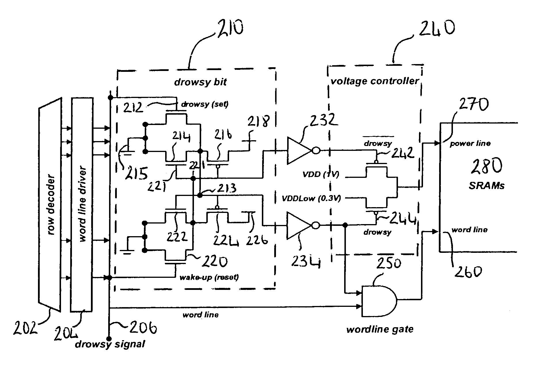
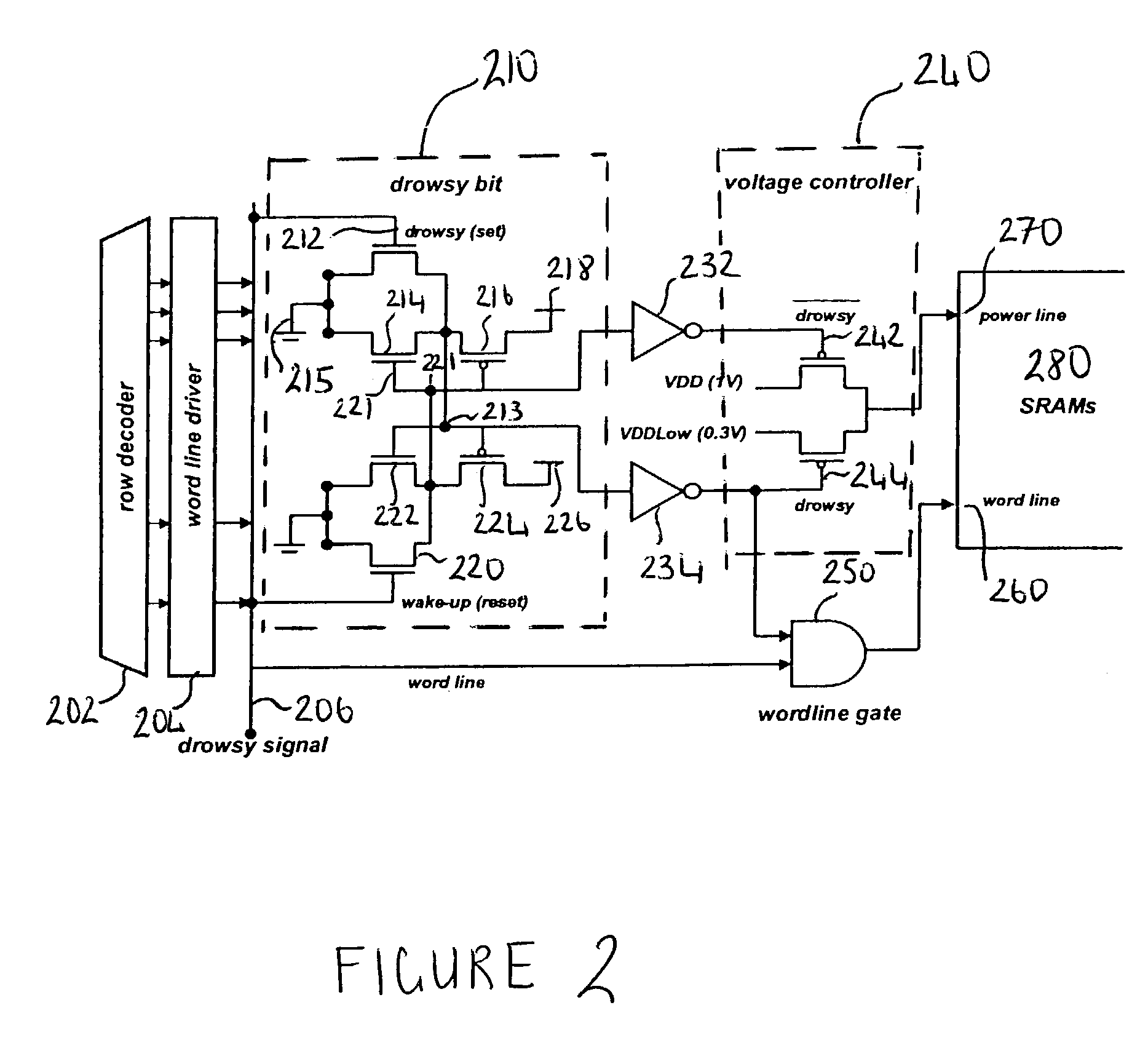
[0072]FIG. 2 schematically illustrates a dynamic voltage scaling (DVS) circuit for a drowsy cache line according to one example embodiment of the invention. The circuit comprises: a row decoder 202; a word line driver 204, a drowsy signal line 206; a drowsy bit control circuit 210 a first NMOS / PMOS series-connected transistor pairs 214, 216 and a second such pair 222, 224, a drowsy (set) NMOS transistor 212 and a wake-up (reset) NMOS transistor 220; a pair of inverter gates 232, 234; a voltage controller comprising two PMOS pass transistors 242 and 244, one of which 242 is connected to a high-voltage line and the other of which 244 is connected to a low-voltage line; a word-line AND gate 250; and an SRAM memory circuit 280 which receives as input a power line270 and a word line 260 from the drowsy bit circuitry.

[0073]The operating voltage of an array of memory cells in SRAM (a cache line) is determined by the voltage controller 240, which switches the array voltage between a high (a...


PUM


Abstract

A memory circuit for use in a data processing circuit is described, in which memory cells have at least two states, each state being determined by both a first voltage level corresponding to a first supply line and a second voltage level corresponding to a second supply line. The memory circuit comprises a readable state in which information stored in a memory cell is readable and an unreadable state in which information stored in said memory cell is reliably retained but unreadable. Changing the first voltage level but keeping the second voltage level substantially constant effects a transition between the readable state and the unreadable state. In use, the static power consumption of the memory cell in the unreadable state is less than static power consumption of the memory cell in the readable state.

Description

[0001]The U.S. Government has a paid-up license in this invention and the right in limited circumstances to require the patent owner to license others on reasonable terms as provided for by the terms of F33615-00-C-1678 awarded by Defense Advanced Research Projects Agency.BACKGROUND OF THE INVENTION[0002]1. Field of the Invention[0003]The present invention relates to memory circuits for data processing. More particularly, this invention relates to reducting static power consumption in such memory circuits.[0004]2. Description of the Prior Art[0005]Complementary metal-oxide semiconductor (CMOS) transistors are the current technology of choice for most data processors due to their advantageous characteristic of consuming power only when switching. When not switching, individual CMOS transistors consume a negligible amount of power (˜10−15 Amps for N-type or P-type transistor) although the cumulative leakage current for modem data processors which have high transistor densities is beco...

Claims


Application Information

Patent Timeline
Patent Type & Authority Patents(United States)
IPC IPC(8): G06F12/00G06F12/08G06F13/00G11C7/20G11C7/22G11C11/417
CPCG06F12/0893G11C5/14G11C5/143G11C5/144G11C7/22G11C8/10G11C8/12G11C11/417G11C7/20G06F2212/1028Y02B60/1225G11C2207/2227Y02D10/00
Inventor FLAUTNER, KRISZTIANBLAAUW, DAVID T.MUDGE, TREVOR N.KIM, NAM S.MARTIN, STEVEN M.
Owner ARM LTD
Why Eureka
Try Eureka