Self-adjusting, adaptive, minimal noise input amplifier circuit

Inactive Publication Date: 2005-03-29
SAMSUNG ELECTRONICS CO LTD
View PDF28 Cites 19 Cited by
  • Summary
  • Abstract
  • Description
  • Claims
  • Application Information

AI Technical Summary

Benefits of technology

In general, the present invention provides a self-adjusting adaptive input circuit with minimal excess noise and a linear charge-handling capacity exceeding 109 electrons to enable high-quality imaging at long wavelength infrared backgrounds and video frame rates. The invention supports various types of photovoltaic and photoconductive detectors, and largely reduces the fixed pattern noise relative to the prior art. The self-adjusting adaptive minimal noise input (SAAMI) amplifier circuit comprises either impedance-buffered or direct injection detector interface with self-nulling skimming of the background signal and self-adapting offset suppression. An integration capacitor stores a charge produced from a photodetector. A self-adjusting current source skims a portion of this charge so that the integration capacitor stores only the differen

Problems solved by technology

The resulting video has large margin over th

Method used


Image

  • Self-adjusting, adaptive, minimal noise input amplifier circuit
  • Self-adjusting, adaptive, minimal noise input amplifier circuit
  • Self-adjusting, adaptive, minimal noise input amplifier circuit

Examples


first embodiment

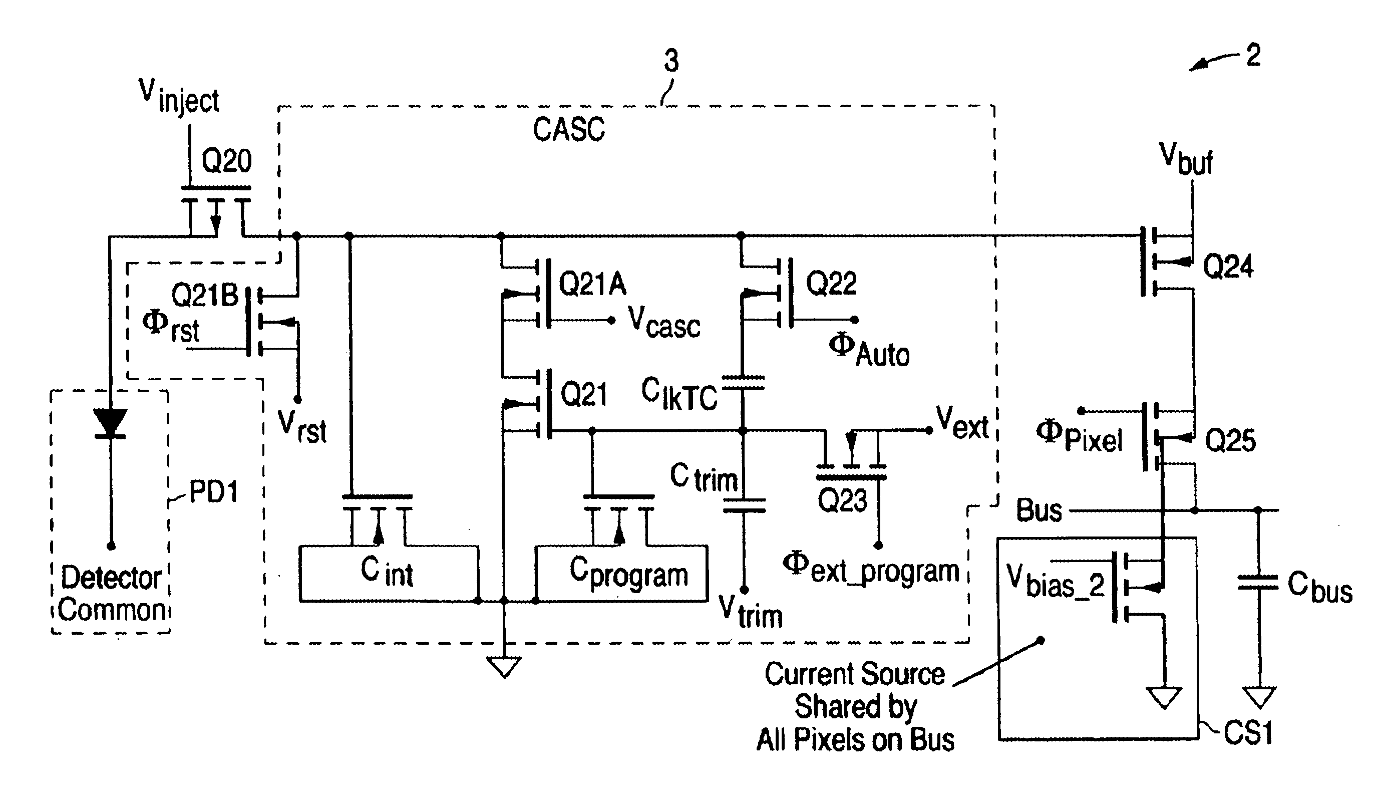
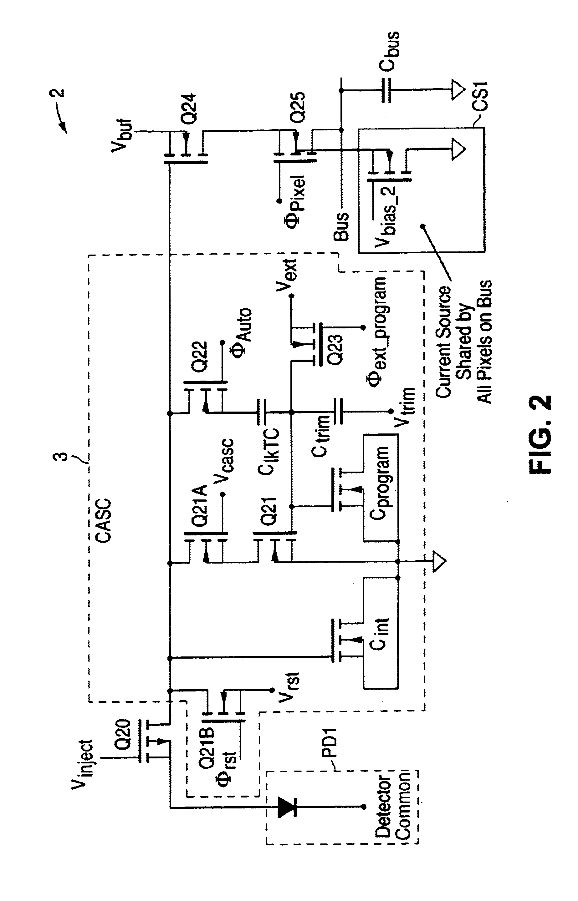
the present invention is shown in FIG. 2. The amplifier circuit 2 comprises a detector PD1 that is directly coupled to the source of an input transistor Q20. The gate of Q20 is adjusted to set the detector bias and the source of Q20 is modulated by the photo-generated signal from PD1. Minority carriers are injected into an integration capacitor Cint where they are accumulated for subsequent readout. This integration capacitor can be reset by a transistor Q21B to an initial voltage Vstore that may even be a large external voltage as taught by U.S. Pat. No. 6,064,431, noted above, or it may be generated on chip. Alternately, other variants can have the integration capacitor tied to a common level or ground.

To enhance the effective integration capacity, the integration capacitor Cint is connected to a self-adjusting current source comprising transistor Q21 (preferably cascoded with transistor Q21A to prevent undesirable parasitic coupling from Cint to the gate of Q21), a programming ca...


PUM


Abstract

A self-adjusting adaptive input circuit with minimal excess noise and a linear charge-handling capacity exceeding 109 electrons to enable high-quality imaging at long wavelength infrared backgrounds and video frame rates is disclosed. An integration capacitor stores a charge produced from a photodetector. A self-adjusting current source skims a current during integration on the integration capacitor. The gate voltage of a skimming transistor is set via a programming transistor in order to set the skim level.

Description

BACKGROUND OF THE INVENTION1. Field of the InventionThe present invention relates generally to interface circuits for focal plane arrays (FPAs) and, specifically, to a self-adjusting adaptive amplifier circuit that uniquely provides high charge-handling capacity for optimally coupling IR detectors to multiplexing readouts in high-density staring FPAs.2. Description of the Related ArtOptical sensors transform incident radiant signals in any spectral wavelength region, but most specifically in the near infrared (NIR; λ=0.8-2 μm), short wavelength IR (SWIR; λ=2.0-2.5 μm), medium wavelength IR (MWIR; λ=2.5-5 μm), and long wavelength IR (LWIR; λ=5-30 μm) bands into electrical signals that are used for data collection, processing, storage and display, such as real-time video. For high-quality imaging of various scenes without concern for ambient light, the MWIR and LWIR bands are often used interchangeably. However, MWIR infrared detector systems typically require sophisticated signal pro...

Claims


Application Information

Patent Timeline
IPC IPC(8): H04N3/15H04N5/33H04N5/363H04N5/374
CPCH04N5/3745H04N5/363H04N25/65H04N25/77
Inventor KOZLOWSKI, LESTER J.TENNANT, WILLIAM E.KLEINHANS, WILLIAM A.
Owner SAMSUNG ELECTRONICS CO LTD
Why Eureka
Try Eureka