Two-dimensional photonic crystal device

a photonic crystal and two-dimensional technology, applied in the field of two-dimensional photonic crystal devices, can solve the problems of bulky optical ics, difficult to fabricate the device of document 1, and high cost of optical communication systems in the internet, and achieve the effect of facilitating fabrication

Inactive Publication Date: 2005-03-29
JAPAN AVIATION ELECTRONICS IND LTD
View PDF4 Cites 18 Cited by
  • Summary
  • Abstract
  • Description
  • Claims
  • Application Information

AI Technical Summary

Benefits of technology

[0015]The resonant pillars are formed of the same medium as that of pillars forming a periodic structure of the two-dimensional photonic crystal, and hence it can be constructed

Problems solved by technology

The WDM technology is now going mainstream in the construction of optical communication networks although the use of expensive WDM components inevitably raises the overall cost of optical communication systems in the Internet.
On the other hand, a low-loss, bend waveguide in optical ICs needs to be gently bent over as long a distance as hundreds of μm—this inevitably makes the optical ICs bulky.
However, in the two-dimensional photonic crystal device of document 1, for example, when the wavelength of light to be propagated is 1.55 μm, the thickness of the wall of the slab 11 between the cavities 16 of the periodic structure and the cavity forming the point defect 1

Method used


Image

  • Two-dimensional photonic crystal device
  • Two-dimensional photonic crystal device
  • Two-dimensional photonic crystal device

Examples


embodiment 1

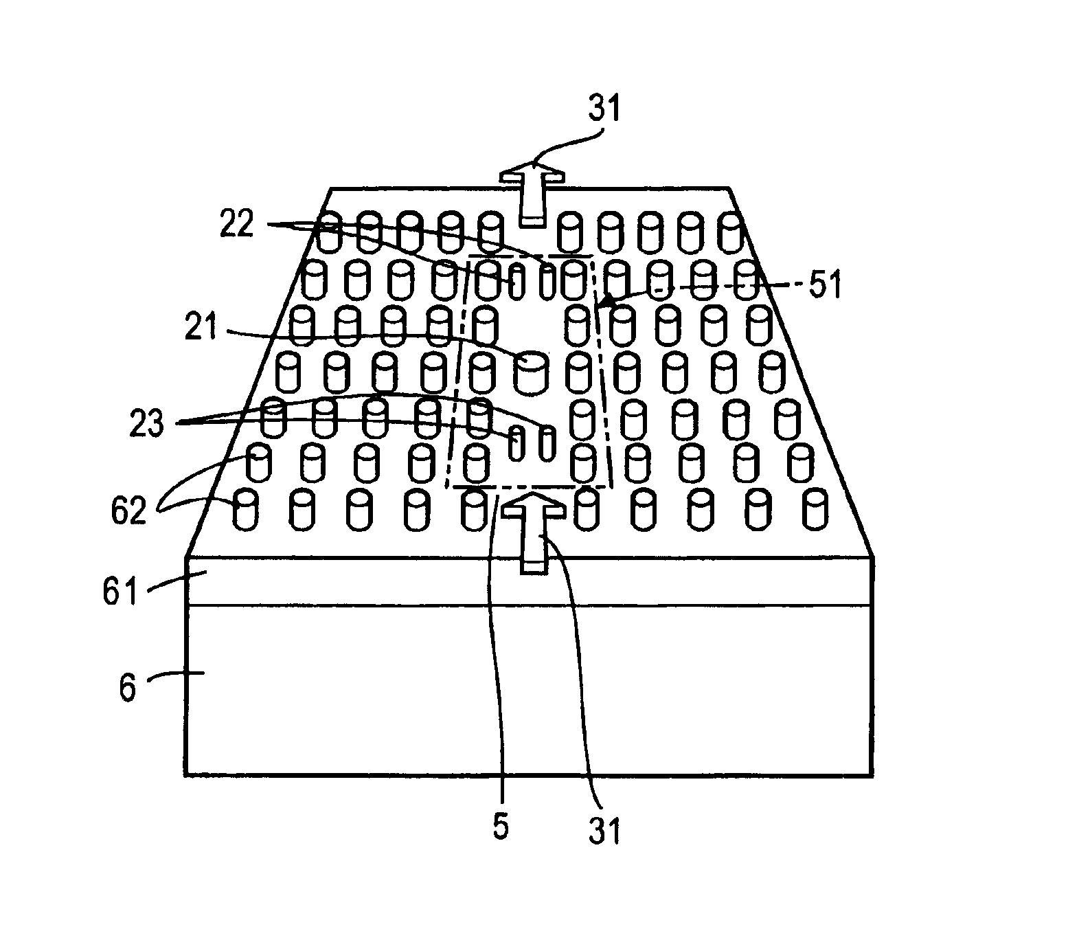
[0070]A description will be given first, with reference to FIGS. 4A and 4B, of the basic structure of a two-dimensional photonic crystal device according to this embodiment. The two-dimensional photonic crystal device of this embodiment is fabricated by forming a SiO2 film 61 over the entire surface of a silicon substrate 6 and patterning a silicon thin film coated all over the SiO2 film 61 by means of lithography and etching to form columnar pillars 62.

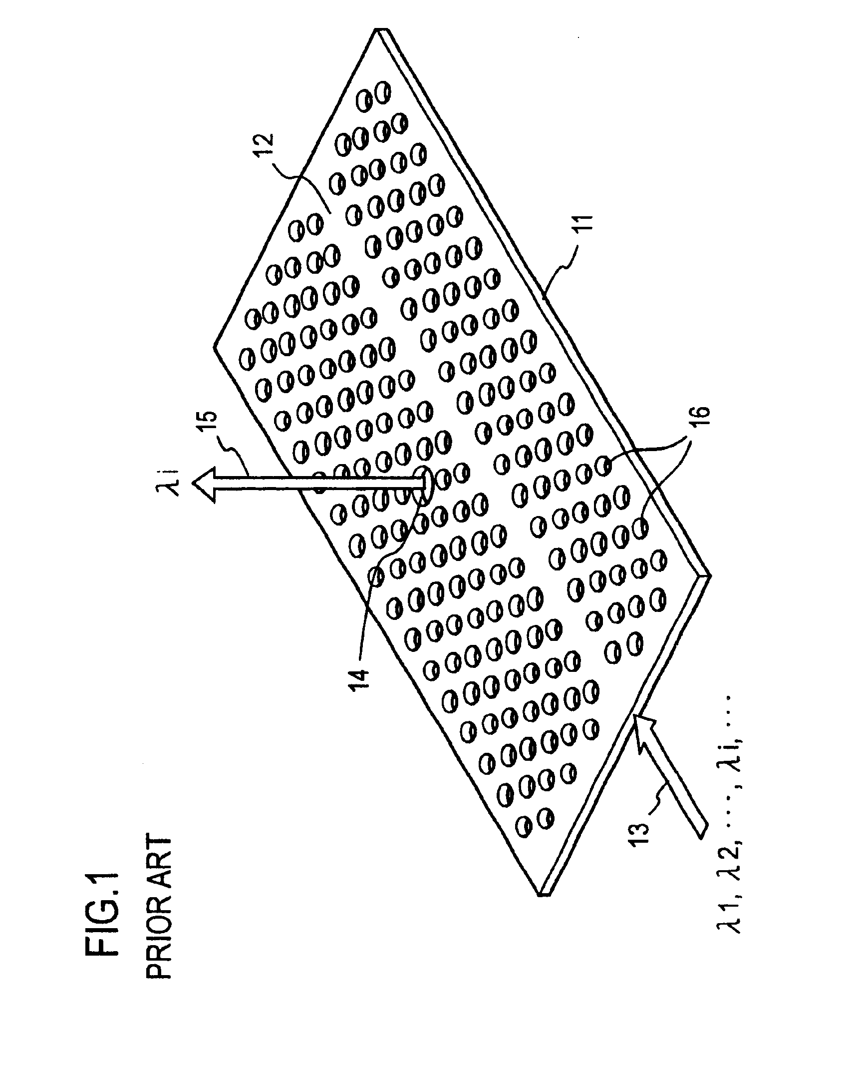
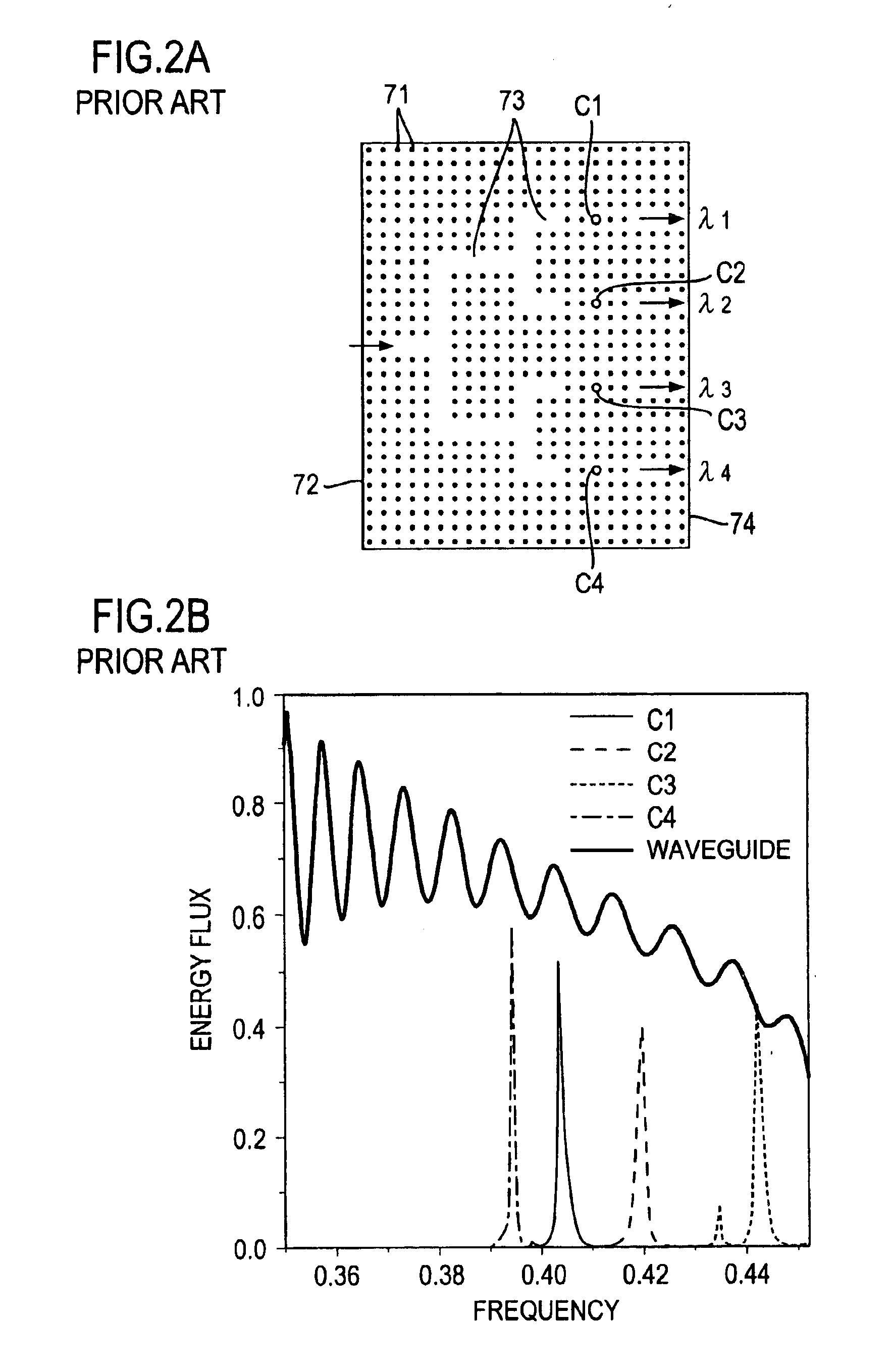
[0071]The columnar pillars 62 formed of silicon are arranged in rows and columns at equal intervals, that is, in a square lattice pattern; a periodic structure of the silicon (with a refractive index of 3.4) pillars 62 arranged in air (with a refractive index of 1.0) constitutes a two-dimensional photonic crystal. The two-dimensional photonic crystal has crystal defects created by the absence of one line of silicon pillars 62; the crystal defects constitute a line waveguide 5, in which there is formed a resonator 51.

[0072]The resonat...

embodiment 2

[0115]In this embodiment the width of the line waveguide is locally narrowed to obtain a high Q-factor and enhance the resonator performance, thereby implementing excellent wavelength selective characteristics. FIGS. 23A and 23B illustrate a basic structure of the two-dimensional photonic crystal device according to this embodiment. The parts corresponding to those in FIGS. 4A and 4B are identified by the same reference numerals, and no detailed description will be repeated.

[0116]In this embodiment, in the area of the waveguide 5 where to form the resonator 51, the pillars of the periodic structure at both sides of the waveguide 5 widthwise thereof are displaced so that the width of the waveguide 5 is narrowed symmetrically in respect of the center line thereof. The displaced pillars 62 are indicated by dots in FIGS. 23A and 23B. In the illustrated example five pillars 62 which define either side of the waveguide 5 widthwise thereof are displaced. The width of the waveguide 5 is nar...


PUM


Abstract

Columnar pillars are arranged in a square lattice pattern to form a two-dimensional photonic crystal. The two-dimensional photonic crystal has crystal defects created by the absence of pillars, and a resonator is formed in a line waveguide provided by the crystal defects. The resonator is made up of a main pillar, a pair of sub-pillars disposed at the light incidence side of the waveguide with respect to the main pillar and another pair of sub-pillars at the light emitting side of the waveguide with respect to the main pillar, the main pillar and sub-pillars being disposed in the waveguide. The main pillar and the sub-pillars are formed of the same medium as that of the pillars, and are formed simultaneously with the pillars by patterning a silicon thin film coated all over a silicon substrate through a SiO2 film formed over the entire surface thereof. Light of a particular wavelength in wavelength-multiplexed incident light is transmitted through the resonator.

Description

BACKGROUND OF THE INVENTION[0002]The present invention relates to a two-dimensional photonic crystal device and, more particularly, to a two-dimensional photonic crystal device for use in WDM (Wavelength Division Multiplex) communications and in similar technical fields.[0003]Over the past few years, spectacular technological advances have been made in the field of optical wavelength division multiplexing (hereinafter referred to as WDM) communications. These technological progresses aim to meet the demands by network users for higher communication speeds in the Internet. The WDM technology is now going mainstream in the construction of optical communication networks although the use of expensive WDM components inevitably raises the overall cost of optical communication systems in the Internet. Nowadays, optics is used in various fields of transmission of information through optical communication networks. The next generation optics is expected as technologies that implement some or...

Claims


Application Information

Patent Timeline
IPC IPC(8): G02B6/12G02B6/122
CPCB82Y20/00G02B6/1225G02B6/12007G02B2006/12164
Inventor BOURELLE, EMMANUEL
Owner JAPAN AVIATION ELECTRONICS IND LTD
Why Eureka
Try Eureka