III group nitride based semiconductor element and method for manufacture thereof
a semiconductor element and group nitride technology, applied in the direction of polycrystalline material growth, crystal growth process, chemically reactive gas, etc., can solve the problem that metal nitride having such a thickness has not been provided as a raw material, and achieves good crystallinity, easy formation, and sufficient stiffness
- Summary
- Abstract
- Description
- Claims
- Application Information
AI Technical Summary
Benefits of technology
Problems solved by technology
Method used
Image

Examples
embodiments
[0057]Embodiments of the invention will be described below.
first embodiment
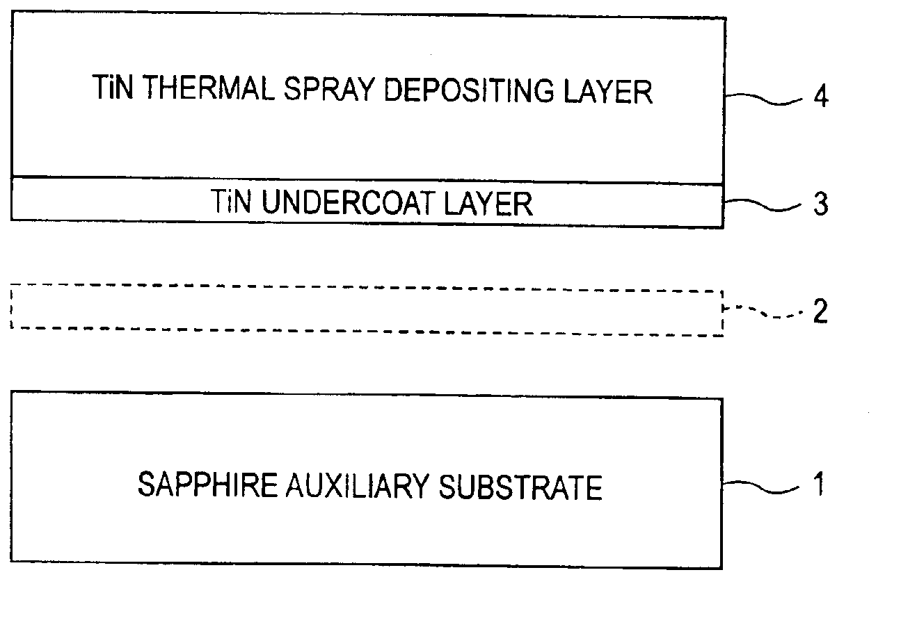
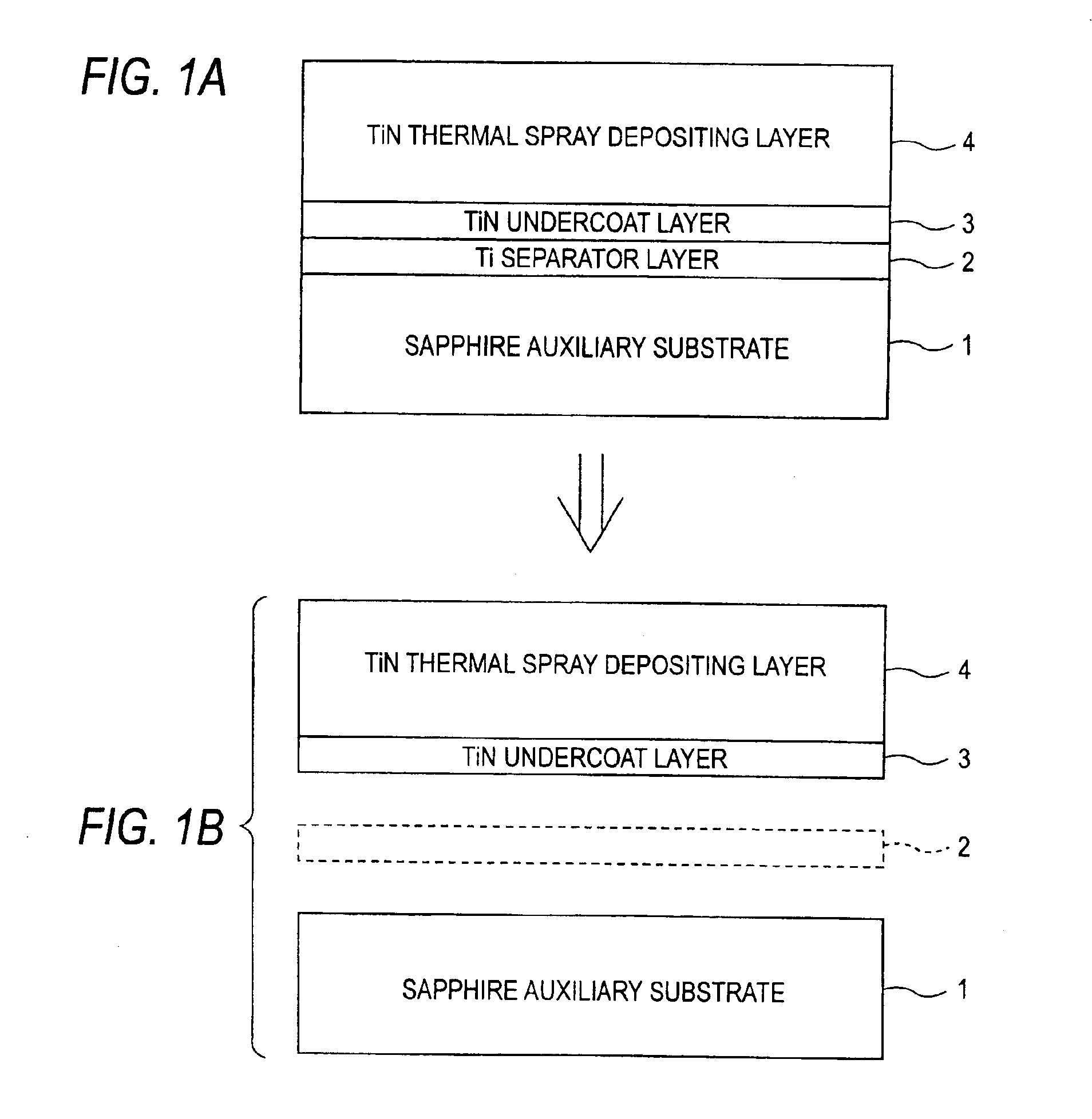
[0058]First, as shown in FIG. 1A, a Ti layer (1 μm) as a separator layer 2 is formed on a sapphire substrate (300 μm) as an auxiliary substrate 1 at a temperature of 450° C. (substrate temperature) by reactive DC magnetron sputtering. Then, a TiN layer (3 μm) as an undercoat layer 3 is formed at a temperature of 450° C. by reactive DC magnetron sputtering in the same manner as described above.
[0059]Then, a TiN thermal spray depositing layer 4 is formed by gas tunnel type plasma reactive spray coating so that the TiN thermal spray depositing layer 4 is 300 μm thick. On this occasion, the substrate temperature is preferably selected to be not higher than 650° C. This because the crystallographic structure of Ti changes at a temperature of not lower than 700° C.
[0060]Then, the resulting substrate is immersed in hydrofluoric acid at 25° C. for about 100 hours so that the Ti separator layer 2 is dissolved as shown in FIG. 1B.
[0061]Then, the thermal spray depositing layer 4 and the underc...
second embodiment
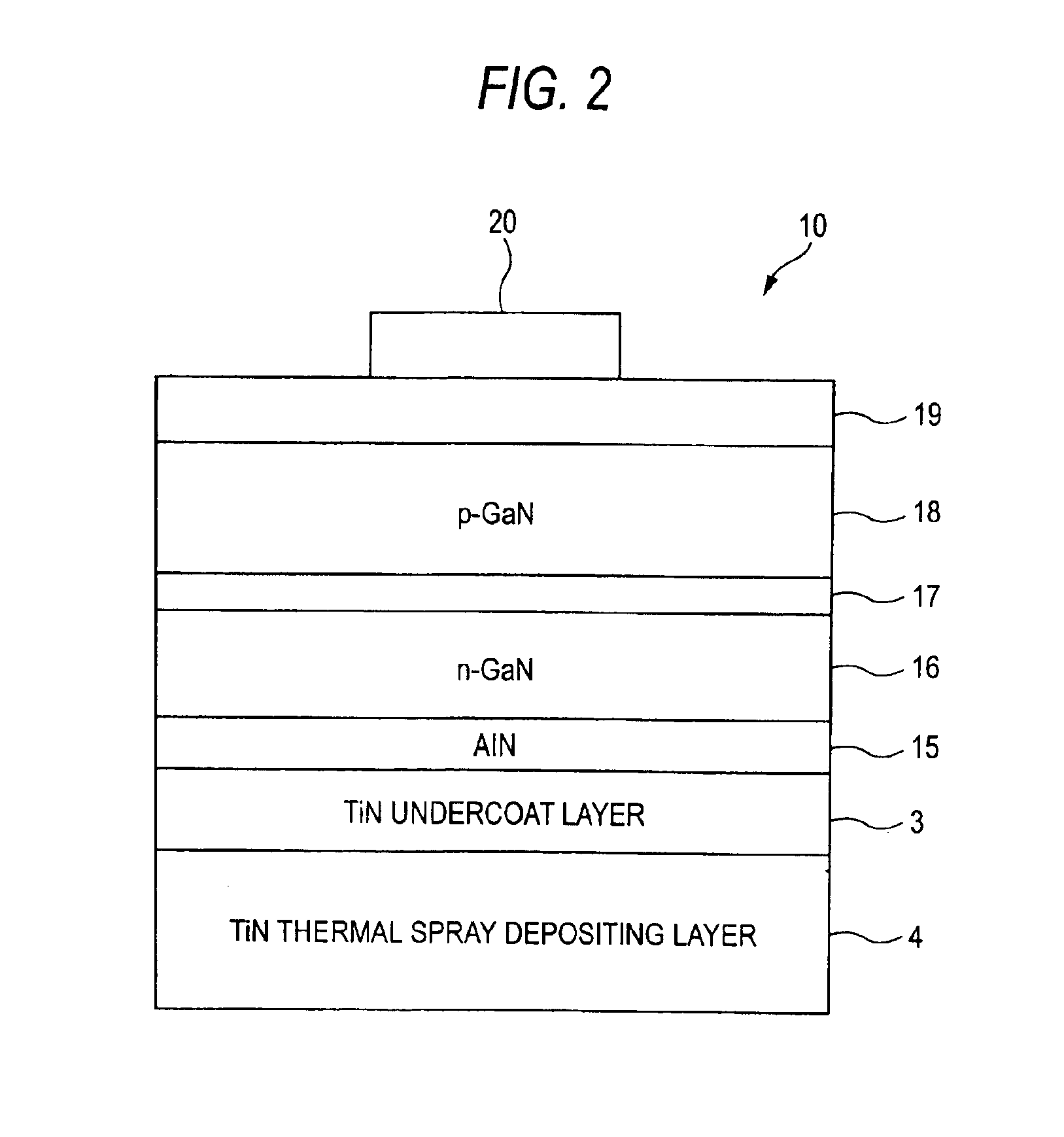
[0075]FIG. 3 shows a semiconductor device according to a second embodiment of the invention. The semiconductor device according to this embodiment is a light-emitting diode 32. Incidentally, parts the same as those in FIG. 2 are denoted by the same reference numerals as those in FIG. 2 for the sake of omission of description.
[0076]Specifications of respective layers are as follows.
LayerCompositionn-type layer 28n-GaN:SiLayer 17 containing acontaining InGaNlight-emitting layerp-type layer 26p-GaN:MgBuffer layer 15AlNUndercoat layer 3TiNThermal spray depositingTiNlayer 4
[0077]As shown in FIG. 3, the p-type layer 26, the layer 17 containing a light-emitting layer and the n-type layer 28 are grown successively on the buffer layer 15 to form a light-emitting diode 32. In the case of the device 32, the light-transmissive electrode (see the reference numeral 19 in FIG. 2) can be dispensed with because the n-type layer 28 low in resistance value forms the uppermost surface.
[0078]In the draw...
PUM
| Property | Measurement | Unit |
|---|---|---|
| Thickness | aaaaa | aaaaa |
| Semiconductor properties | aaaaa | aaaaa |
Abstract
Description
Claims
Application Information
 - Generate Ideas
- Intellectual Property
- Life Sciences
- Materials
- Tech Scout
- Unparalleled Data Quality
- Higher Quality Content
- 60% Fewer Hallucinations
Browse by: Latest US Patents, China's latest patents, Technical Efficacy Thesaurus, Application Domain, Technology Topic, Popular Technical Reports.
© 2025 PatSnap. All rights reserved.Legal|Privacy policy|Modern Slavery Act Transparency Statement|Sitemap|About US| Contact US: help@patsnap.com