Automated approach to constraint generation in IC design

a constraint generation and automatic approach technology, applied in the field of integrated circuit (ic) design, can solve the problems of new challenges in ic design, schedule slippage, additional r&d costs, etc., and achieve the effects of reducing the risk of design iterations, reducing the risk of design failure, and realistic block timing budgets

Inactive Publication Date: 2005-04-05
FISHTAIL DESIGN AUTOMATION
View PDF2 Cites 30 Cited by
  • Summary
  • Abstract
  • Description
  • Claims
  • Application Information

AI Technical Summary

Benefits of technology

The Focus system, as summarized above, provides significant advantages in IC design, by providing:A reduction in the risk of design failures by providing engineers an early understanding of the precise challenges they face in realizing a design. By providing virtual-prototyping tools with golden timing constraints, the Focus system empowers the tools to create more realistic block timing budgets. Correct block implementation constraints, in turn, reduce the risk of design iterations.A reduction in the cost and power consumption of a design. By generating timing constraints that do not over-constrain a design, the Focus system allows block implementation tools to generate circuits that consume as little area and power as possible, while meeting performance objectives. Reduction in IC area typically translates to a reduction in unit costs. Reduction in power consumption is crucial for several consumer products.A reduction in IC design time by automating a task that is central to IC design. Engineers conventionally specify timing constraints in an ad-hoc and continually evolving manner. As timing problems are uncovered, and most of them tend be uncovered late in the implementation flow, exceptions to single-cycle clocking are inserted. All of this takes time, is error-prone and is the source of much anxiety during IC sign-off.The Focus system empowers an RTL-handoff-based design flow. With the Focus system, system design houses are able to describe the design they want to implement and hand this design, along with its constraints, to a semiconductor vendor that will take responsibility for implementing the design to meet requirements. Semiconductor vendors typically prefer RTL handoff because it allows them to take responsibility for a greater portion of the design flow. System design houses prefer RTL handoff because it allows them to focus on their core competency, which is the design of compelling products.

Problems solved by technology

As need for density and speed steadily increase, new challenges arise in IC design.
Still, even in the face of the complexity of the task, small market windows and short product lifecycles provide no room for error in the execution of chip design projects—schedule slippage is measured not just in terms of additional R&D costs, but in lost market opportunities that can be fatal for a company.
Integrated circuit designers are therefore under tremendous pressure to design complex chips to meet design and marketing requirements.
The feasibility of a design, however, hinges on whether these delays are actually within acceptable bounds.
Without good constraints on the permissible delays for the millions of timing paths on a chip, virtual prototyping tools are insufficient to gauge actual design feasibility.
Absence of good timing constraints early in the design flow also results in chip implementation tools (logic synthesis, place & route) being asked to meet requirements that are both unnecessarily stringent and uncertain.
This severely impacts ability of such tools to generate low-cost, low-power implementations that meet performance requirements without requiring design iterations.

Method used


Image

  • Automated approach to constraint generation in IC design
  • Automated approach to constraint generation in IC design
  • Automated approach to constraint generation in IC design

Examples


Embodiment Construction

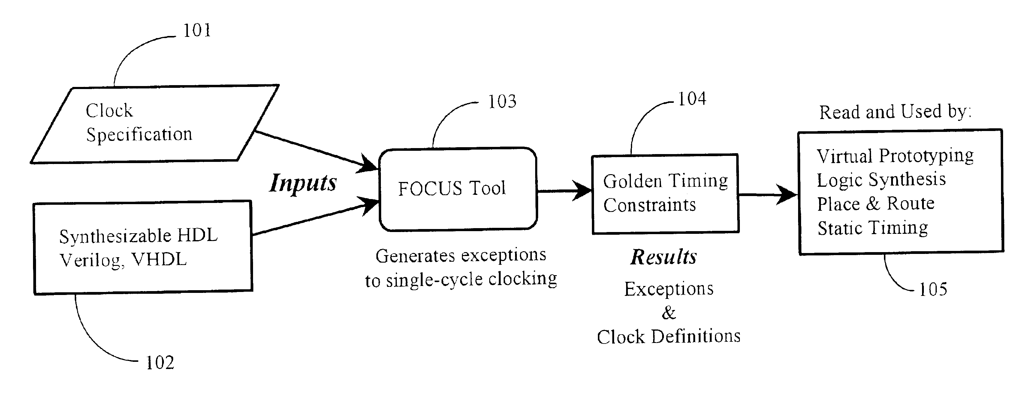
The system of the present invention, in a preferred embodiment, is a software-enabled system that automatically (i.e. without user-specified stimulus), analyzes a cycle-accurate description of interaction among functional blocks on a proposed IC, to generate timing constraints that must be satisfied by the IC to meet design requirements.

It is well-known that there are, broadly speaking, two historically distinct stages in the creation of a new IC: (1) the design stage, and (2) the implementation stage. The system of the invention, termed Focus by the inventors, links the two stages for the first time by establishing constraints imposed on the implementation stage by facts and characteristics of the design stage.

It is well-known that development engineers constrain the delays on the timing paths of a proposed IC based on the speed at which they intend to clock the IC. The engineers specify the clocks on their design and every timing path on the IC is required to have a delay less tha...


PUM


Abstract

A software-based system for generating timing constraints for a proposed IC design has a first input as a synthesizable description of the proposed IC, a second input as a clock specification for the proposed IC, and a processing unit accepting the first and second inputs, and determining therefrom as an output, a set of timing constraints to guide implementation of the proposed IC design.

Description

FIELD OF THE INVENTIONThe present invention is in the technical area of integrated circuit (IC) design, and pertains more specifically to Electronic Design Automation (EDA) tools providing methods and apparatus for generating timing constraints in a design project.BACKGROUND OF THE INVENTIONThe term integrated circuit (IC) is a very general term covering a very broad range of electronic devices based on solid-state electronics, such as microprocessors. It is now notoriously well-known that a vast array of consumer products, especially those products in the area of telecommunications and computerized devices (including personal computers), are based on ICs, such as central processing units (CPUs), microprocessors, and, of course, digital memory devices of many sorts.In the art of IC design and manufacturing, ongoing research and development in a highly competitive environment is conducted to produce new and better devices, which are manufactured by usually well-know techniques involv...

Claims


Application Information

Patent Timeline
Patent Type & Authority Patents(United States)
IPC IPC(8): G06F17/50
CPCG06F17/5045G06F2217/06G06F2111/04G06F30/30
Inventor DAGA, AJAY JANAMI
Owner FISHTAIL DESIGN AUTOMATION
Why Eureka
Try Eureka