Method to solve via poisoning for porous low-k dielectric

a low-k dielectric and porous technology, applied in the field of manufacturing of semiconductor devices, can solve the problems of poisoning of vias, poor interfaces between contact conductors, and poisoning of interconnects or vias, and achieve the effect of preventing outgassing

Inactive Publication Date: 2005-04-12
TAIWAN SEMICON MFG CO LTD
View PDF8 Cites 50 Cited by
  • Summary
  • Abstract
  • Description
  • Claims
  • Application Information

AI Technical Summary

Benefits of technology

It is another object of the present invention to provide a method of forming a protective layer on an around low-k porous dielectric materials to prevent outgassing and the attendant via poisoning when forming copper vias in them.
It is yet another object of the present invention to provide a method of forming dual damascene structures without via poisoning when formed in low-k porous dielectric materials.

Problems solved by technology

However, low-k dielectrics are usually porous, and can trap moisture and other contaminants, thereby giving rise to poisoned interconnects, or vias, as is known in the art, during the process of manufacturing integrated circuit chips.
However, if the damascene structure is not properly protected during forming of the contact and via holes, the holes can be “poisoned” due to outgassing from the insulative layers, and / or due to the hydrophobic nature of the insulative layers.
A poisoned contact hole (reaching the substrate), or a poisoned via hole (connecting different metallized layers) can give rise to voids, cavities for contaminants to enter, poor interfaces between contacting conductors, and, hence, poor connections between interconnects.
As the feature sizes get smaller, the smaller geometries result in higher electrical resistances, which in turn degrade circuit performance.
This moisture diffuses into the metal causing poisoned via / contact metallurgy.

Method used


Image

  • Method to solve via poisoning for porous low-k dielectric
  • Method to solve via poisoning for porous low-k dielectric
  • Method to solve via poisoning for porous low-k dielectric

Examples


Embodiment Construction

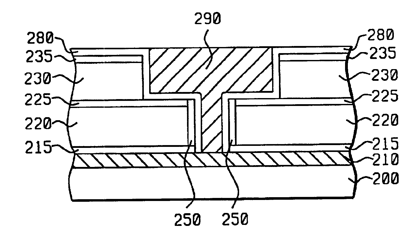
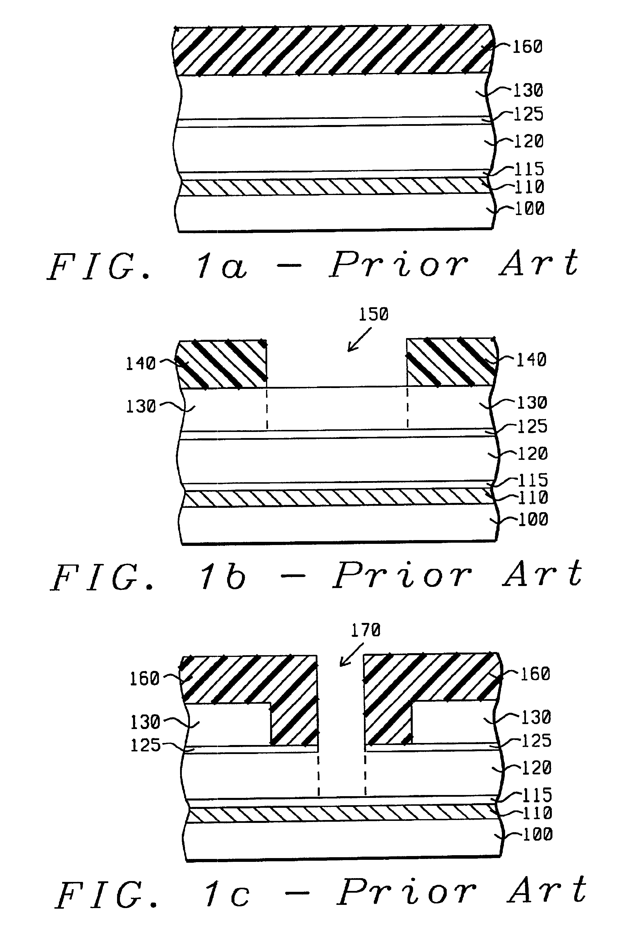
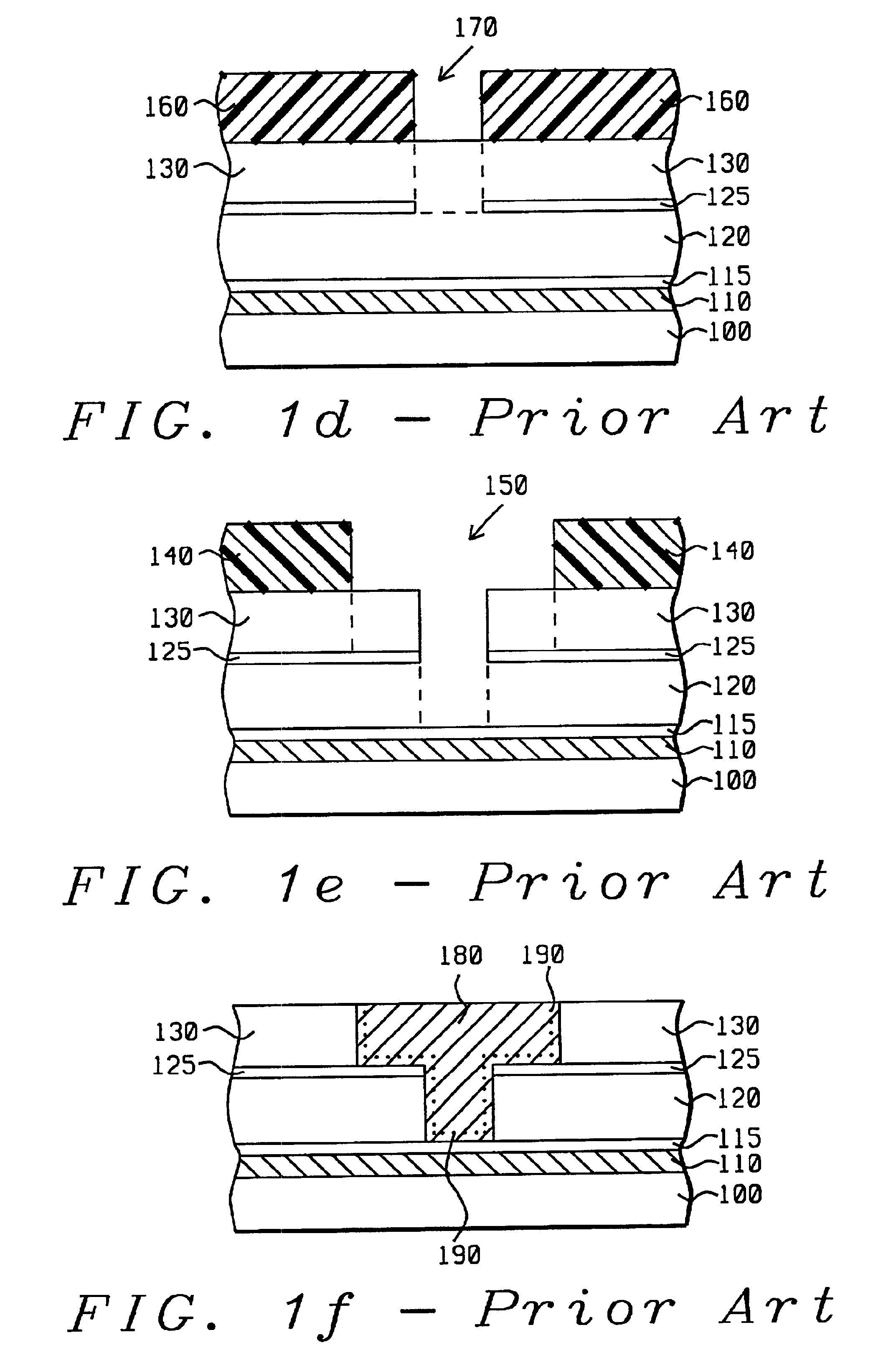
Referring now the drawings, FIGS. 2a-2i, there is shown a method of reducing via poison in low-k Cu dual damascene structures through a protective layer that is formed. It will be apparent to those skilled in the art that the disclosed method will be especially suitable for porous low-k dielectric materials in which a single via or a dual damascene structure is formed. This is because, the protective layer that is disclosed prevents any outgassing from the porous low-k dielectric layer that may have harbored moisture and impurities during the earlier various process steps, and any detrimental effects thereof during the subsequent steps of depositing metal in the single or the dual damascene structure.

Specifically, FIG. 2a shows a portion of a semiconductor substrate (200), which is preferably silicon. In FIG. 2a, the substrate is provided with first metal layer (210) and a passivation layer (215). Metal is preferably copper with a thickness between about 1000 to 10000 Å, and the pas...


PUM

PropertyMeasurementUnit
dielectric constantaaaaaaaaaa
dielectric constantsaaaaaaaaaa
temperatureaaaaaaaaaa

Abstract

A method of forming a via in a low-k dielectric material and without the attendant via poisoning problem, or a dual damascene structure formed in the same dielectric and without the same problem are disclosed. The vertical walls of the via opening are first lined with a low-k protection layer and then covered with a barrier layer in order to prevent outgassing from the low-k dielectric material when copper is deposited into the via opening. In the case of a dual damascene structure, it is sufficient that the hole opening underlying the trench opening is first lined with the low-k protection layer. The resulting via or dual damascene structure is free of poisoned metal and, therefore, more reliable.

Description

BACKGROUND OF THE INVENTION(1) Field of the InventionThe present invention relates to the manufacture of semiconductor devices in general, and in particular, to a method of reducing via poisoning in low-k dielectric materials through the use of a protective metal layer.(2) Description of the Related ArtLow-k dielectric materials are favored in the semiconductor industry because they have low dielectric constant (k), and therefore, are useful in reducing the resistance-capacitance (RC) delay, or, time constant, of the circuitry in which they are used. However, low-k dielectrics are usually porous, and can trap moisture and other contaminants, thereby giving rise to poisoned interconnects, or vias, as is known in the art, during the process of manufacturing integrated circuit chips. The present invention discloses a method of preventing such poisoned vias.Copper dual damascene is a preferred interconnect because, as is well known in the art, copper has lower resistivity than the commo...

Claims


Application Information

Patent Timeline
Patent Type & Authority Patents(United States)
IPC IPC(8): H01L21/70H01L21/768
CPCH01L21/76807H01L21/76844H01L21/76831H01L2221/1063
Inventor TSAI, MING-HSINGLIN, JING-CHENGSHUE, SHAU-LINYU, CHEN-HUA
Owner TAIWAN SEMICON MFG CO LTD
Why Eureka
Try Eureka