Nanostructure and nanocomposite based compositions and photovoltaic devices

a technology of nanocomposites and compositions, applied in the field of nanostructures, can solve the problems of marginally better than 10%, low efficiency, and low efficiency of devices, and achieve the effect of improving device efficiency

Inactive Publication Date: 2005-04-12
NANOSYS INC
View PDF51 Cites 598 Cited by
  • Summary
  • Abstract
  • Description
  • Claims
  • Application Information

AI Technical Summary

Benefits of technology

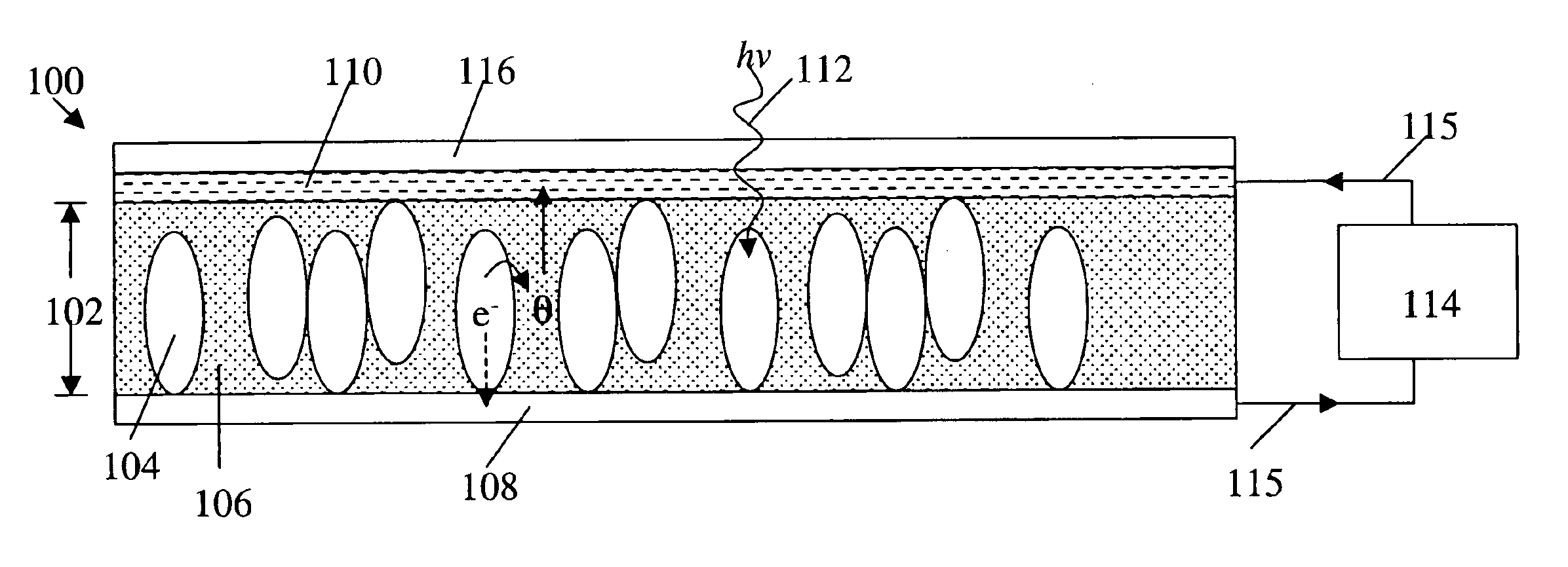
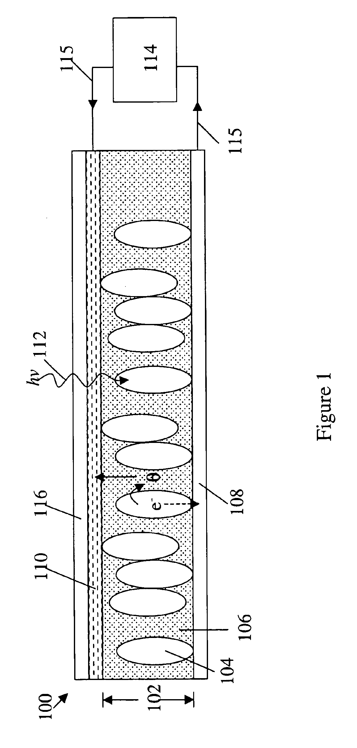
The overall architecture of the device can be selected based upon the use to which the device is to be put. For example, the overall device can comprise a planar or a non-planar architecture. For example, the device optionally comprises a convex architecture to enhance efficiency of the device in settings where convex architecture is desired. Similarly, in one embodiment, the first electrode layer, the photoactive layer and the second electrode layer are optionally oriented in a coiled architecture, or in a reciprocating stacked architecture.

Problems solved by technology

While these devices are useful in certain applications, their efficiency has been somewhat limited, yielding conversion efficiencies, e.g. solar power to electrical power, of typically marginally better than 10%.
While efficiencies of these devices have been improving through costly improvements to device structure, it is believed that physical limitations on these devices mean they will, at best, achieve a maximum efficiency of around 30%.
For ordinary energy requirements, e.g., public consumption, the relative inefficiency of these devices, combined with their relatively high cost, when compared to other means of energy generation, have combined to inhibit the widespread adoption of solar electricity in the consumer markets.
For example, because of their relative inefficiency, as well as their rigid construction, photovoltaic systems typically require adequate flat space that has appropriate sun exposure at all times, or at least during peak times, to meet the requirements for electricity for which the system is used.

Method used


Image

  • Nanostructure and nanocomposite based compositions and photovoltaic devices
  • Nanostructure and nanocomposite based compositions and photovoltaic devices
  • Nanostructure and nanocomposite based compositions and photovoltaic devices

Examples


example 1

Nanocomposite Photovoltaic Device

This example describes fabrication of a CdSe nanocrystal-P3HT polymer nanocomposite photovoltaic device. CdSe nanorods have been used; CdSe nanotetrapods can also be used, as can other nanostructure types and / or compositions.

Substrate Cleaning

Substrates (e.g., ITO on glass, from Thin Film Devices, Inc., www.tfdinc.com) are cleaned, e.g., using the following procedure. Substrates are wiped with isopropanol, ultrasonicated in isopropanol, ultrasonicated in 2% Hellmanex™ deionized water, rinsed very thoroughly under flowing deionized water, ultrasonicated in deionized water, ultrasonicated in semiconductor grade acetone, and ultrasonicated in semiconductor grade isopropanol. Each sonication is for 15 minutes. The substrates are then oxygen plasma cleaned, at 200 W (1% reflected power) for 10 minutes with oxygen introduced at a pressure of approximately 400 mTorr into a vacuum of 80 mTorr.

PEDOT Layer Processing

PEDOT / PSS Poly(3,4-ethylenedioxythiophene) p...

example 2

CdSe—CdTe Nanocrystal Photovoltaic Device

This example describes fabrication of a photovoltaic device comprising two intermixed populations of nanocrystals, CdSe nanocrystals and CdTe nanocrystals.

Substrate Cleaning

Substrates (e.g., ITO on glass, from Thin Film Devices, Inc., www.tfdinc.com) are cleaned, e.g., using the following procedure. Substrates are wiped with isopropanol, ultrasonicated in isopropanol, ultrasonicated in 2% Hellmanex™ deionized water, rinsed very thoroughly under flowing deionized water, ultrasonicated in deionized water, ultrasonicated in semiconductor grade acetone, and ultrasonicated in semiconductor grade isopropanol. Each sonication is for 15 minutes. The substrates are then oxygen plasma cleaned, at 200 W (1% reflected power) for 10 minutes with oxygen introduced at a pressure of approximately 400 mTorr into a vacuum of 80 mTorr.

PEDOT Layer Processing

PEDOT / PSS Poly(3,4-ethylenedioxythiophene) poly(styrenesulfonate) (e.g., Baytron® P VP AI 4083 from H. C. ...


PUM

PropertyMeasurementUnit
aspect ratioaaaaaaaaaa

Abstract

Nanocomposite photovoltaic devices are provided that generally include semiconductor nanocrystals as at least a portion of a photoactive layer. Photovoltaic devices and other layered devices that comprise core-shell nanostructures and/or two populations of nanostructures, where the nanostructures are not necessarily part of a nanocomposite, are also features of the invention. Varied architectures for such devices are also provided including flexible and rigid architectures, planar and non-planar architectures and the like, as are systems incorporating such devices, and methods and systems for fabricating such devices. Compositions comprising two populations of nanostructures of different materials are also a feature of the invention.

Description

FIELD OF THE INVENTIONThe present invention is in the field of nanostructures. More particularly, the invention provides devices, such as photovoltaic devices, comprising nanostructures, which optionally are part of a nanocomposite. Compositions comprising two populations of nanostructures of different materials are also features of the invention, as are methods of and systems for producing photovoltaic and other (e.g., layered) devices.BACKGROUND OF THE INVENTIONSolar energy has long been looked to as a potential solution to the ever increasing energy needs of the planet's population. Increasing costs of mining fossil fuels, increased concerns over “greenhouse” emissions, and increasing instabilities in regions that house large reserves of fossil fuels have furthered interest in exploiting alternative energy strategies, including solar energy sources.To date, solar energy conversion has generally relied upon either the direct harvesting of solar thermal energy, e.g., in heating app...

Claims


Application Information

Patent Timeline
Patent Type & Authority Patents(United States)
IPC IPC(8): H01L31/0264H01L31/036H01L31/00H01L31/04B82B1/00H01LH01L31/0256H01L31/0272H01L31/0296H01L31/0352H01L31/0384H01L51/00H01L51/42
CPCB82Y10/00B82Y20/00B82Y30/00H01L31/0384H01L31/04H01L51/4213H01L51/4226H01L51/426Y02E10/549H01L51/0037H01L51/0036Y02P70/50H10K85/1135H10K85/113H10K30/151H10K30/10H10K30/35
Inventor SCHER, ERIKBURETEA, MIHAI A.CHOW, CALVINEMPEDOCLES, STEPHENMEISEL, ANDREASPARCE, J. WALLACE
Owner NANOSYS INC
Why Eureka
Try Eureka