Laser processing

a laser and laser pulse technology, applied in the field of laser processing, can solve the problems of limited silicon temperature rise, and achieve the effect of improving the overall result in the throughput of successful repair and high repetition rate of laser pulses

Inactive Publication Date: 2005-04-12
ELECTRO SCI IND INC
View PDF30 Cites 82 Cited by
  • Summary
  • Abstract
  • Description
  • Claims
  • Application Information

AI Technical Summary

Benefits of technology

By so limiting the duration in which the energy required to produce link removal is delivered, temperature rise in the silicon can be limited to prevent damage.
According to another aspect of the invention, an optical system is employed to accurately focus a laser spot when operating at a wavelength that is not beyond the absorption edge and the same optical system is used, without modification, at a wavelength beyond the absorption edge, constrained less than 1.2 μm. This provides a versatile new laser system that can be inexpensively retrofitted into existing laser systems. For instance, the initial 1.064 μm laser beam output of the system is useful directly for processing conventional polysilicide or polysilicon links, and, with the same optical system, using the constrained wavelength range beyond the silicon absorption edge, but less than 1.2 μm, fine metal links can be processed. Depending upon the work load of the particular production facility the optics of the system are optimized at one or the other of the working wavelengths.

Problems solved by technology

By so limiting the duration in which the energy required to produce link removal is delivered, temperature rise in the silicon can be limited to prevent damage.

Method used


Image

  • Laser processing
  • Laser processing
  • Laser processing

Examples


Embodiment Construction

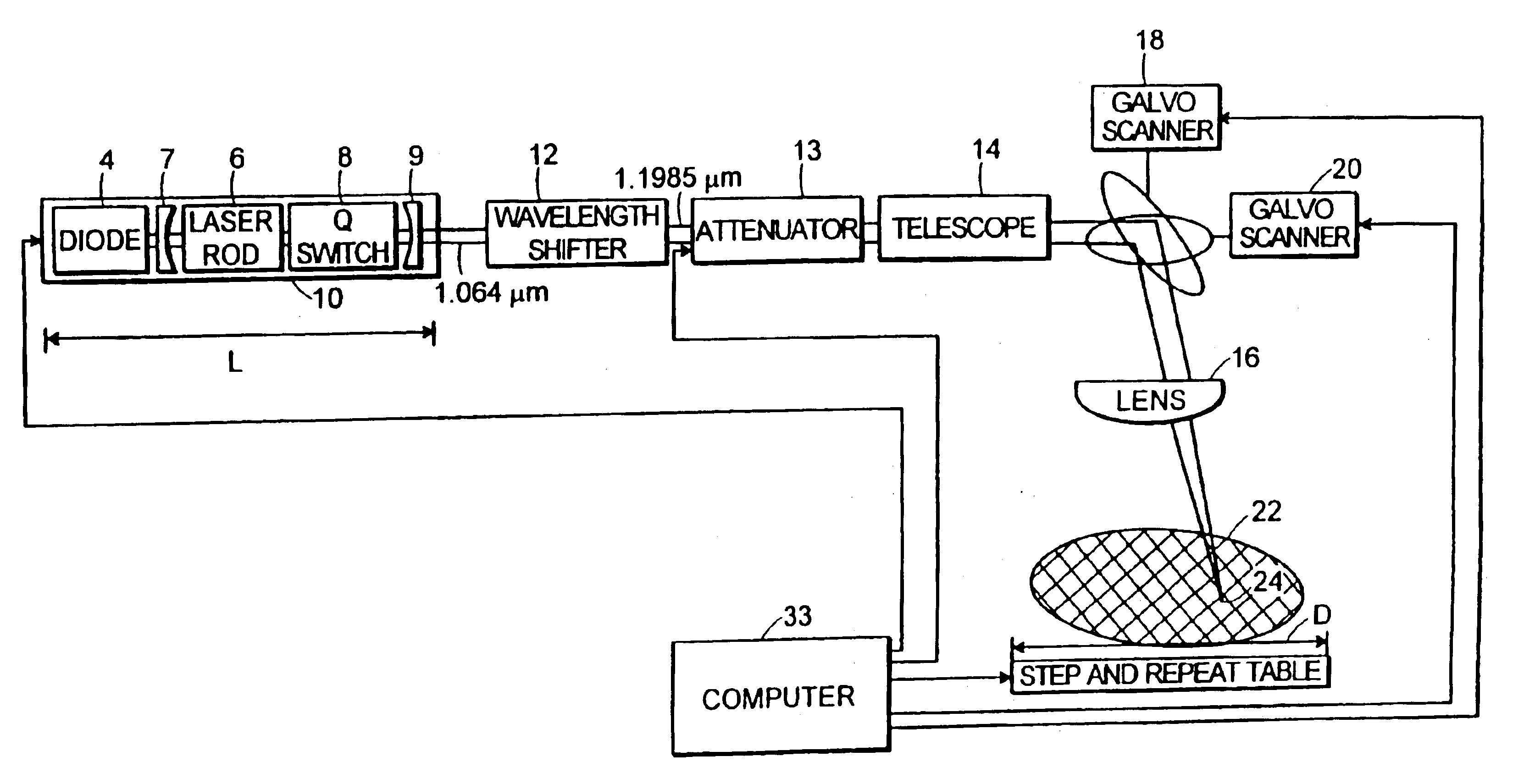
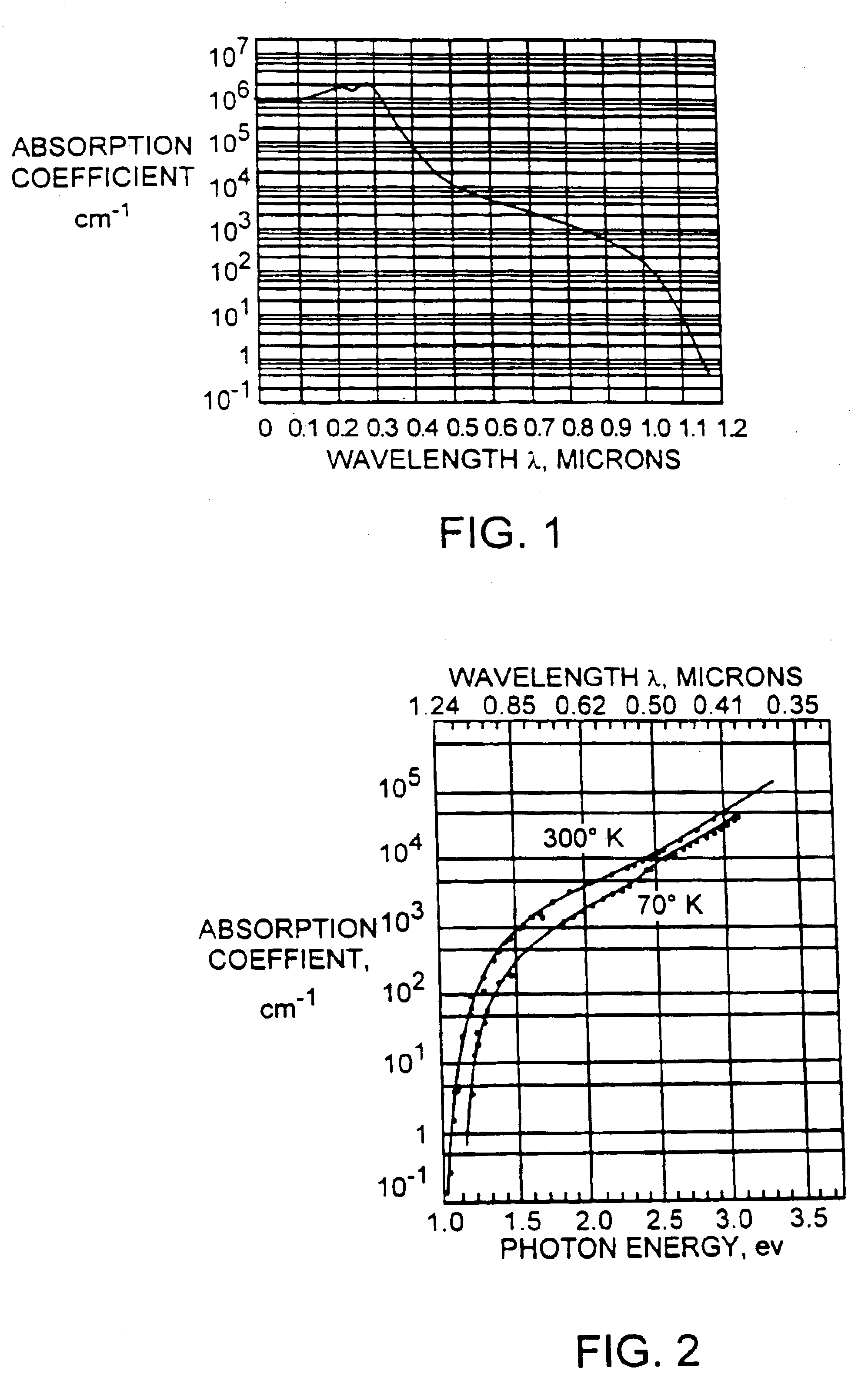
The techniques of the present invention provide quick and reliable removal of links in semiconductor memory devices. By increasing the probability of success of removing individual links, the invention increases the overall probability of successfully repairing a given semiconductor device having many links to be removed, thereby providing successful yields of repaired semiconductor devices.

This is especially important because as the number and density of memory cells in semiconductor devices has increased from 64-kilobit memories to 256-megabit memories, the physical size of the memories has become greater. Although clean rooms have improved, the defect density remains constant for each class of clean room. This means that the number of defects per semiconductor device increases with area. Hence, as the number of storage bits increases, the number of redundant rows and columns of memory also increases. For some 1-megabit memory designs the number of links to support redundant repai...


PUM

PropertyMeasurementUnit
wavelengthaaaaaaaaaa
laser wavelengthaaaaaaaaaa

Abstract

A controlled, switched laser system for vaporizing a target structure on a substrate includes a diode-pumped, solid-state laser for producing a laser output, a controllable switch for controlling the on / off state and power level of the laser, and a wavelength shifter. The wavelength shifter shifts the wavelength of the laser output from a conventional wavelength to a wavelength beyond the absorption edge of the substrate but shorter than 1.2 μm in order to obtain a decrease in absorption of the laser output by the substrate due to the shift in the wavelength of the laser output. The wavelength shifter is removably insertable into the switched laser system so as to enable the switched laser system to operate at the conventional wavelength and at the wavelength beyond the absorption edge of the substrate. Heating of the substrate and hence damage to the substrate is limited due to the wavelength being beyond the absorption edge of the substrate. Good depth of focus of the laser beam output is maintained relative to spot size of the laser beam output due to the wavelength being less than about 1.2 μm.

Description

BACKGROUND OF THE INVENTIONThis invention relates to employing a laser beam to vaporize or otherwise alter a portion of a circuit element on a silicon substrate and is particularly applicable to vaporizing metal, polysilicide and polysilicon links for memory repair.Semiconductor devices such as memories typically have conductive links adhered to a transparent insulator layer such as silicon oxide, which is supported by the main silicon substrate. During laser processing of such semiconductor devices, while the beam is incident on the link or circuit element, some of the energy also reaches the substrate. Depending upon the power of the beam, length of time of application of the beam, and other operating parameters, the silicon substrate can be overheated and damaged.Laser processes of this kind have typically been conducted at wavelengths of 1.047 μm or 1.064 μm. Silicon has sufficiently low absorption at these wavelengths that the amount of beam energy employed to evaporate typical...

Claims


Application Information

Patent Timeline
Patent Type & Authority Patents(United States)
IPC IPC(8): B23K26/40B23K26/00B23K26/06H01L21/70H01L21/768
CPCB23K26/063B23K26/0807B23K26/0853B23K26/365H01L21/76894B23K26/4065B23K26/407B23K26/4075B23K26/4005B23K2201/40B23K26/40B23K26/0622B23K26/082B23K26/361B23K2101/40B23K2103/42B23K2103/50
Inventor SMART, DONALD V.
Owner ELECTRO SCI IND INC
Why Eureka
Try Eureka