Methods and structures for metal interconnections in integrated circuits

a technology of integrated circuits and metal interconnections, which is applied in the direction of semiconductor devices, electrical equipment, semiconductor/solid-state device details, etc., can solve the problems of increasing the cost of manufacturing integrated circuits, wasting power, and wasting power, so as to achieve faster, more-efficient integrated circuits, and eliminate trench digging steps

Inactive Publication Date: 2005-04-12
ROUND ROCK RES LLC
View PDF120 Cites 16 Cited by
  • Summary
  • Abstract
  • Description
  • Claims
  • Application Information

AI Technical Summary

Benefits of technology

Thus, the method of the present invention yields a self-planarizing metallic structure that not only eliminates the time-consuming, trench-digging ste...

Problems solved by technology

Current interconnection techniques suffer from two significant shortcomings.
First, because of limitations in the photolithography used to define metallization patterns, current techniques require digging trenches to ensure that deposited metallic lines are flush, or coplanar, with the surface of the underlying insulation.
Howeve...

Method used


Image

  • Methods and structures for metal interconnections in integrated circuits
  • Methods and structures for metal interconnections in integrated circuits
  • Methods and structures for metal interconnections in integrated circuits

Examples


Embodiment Construction

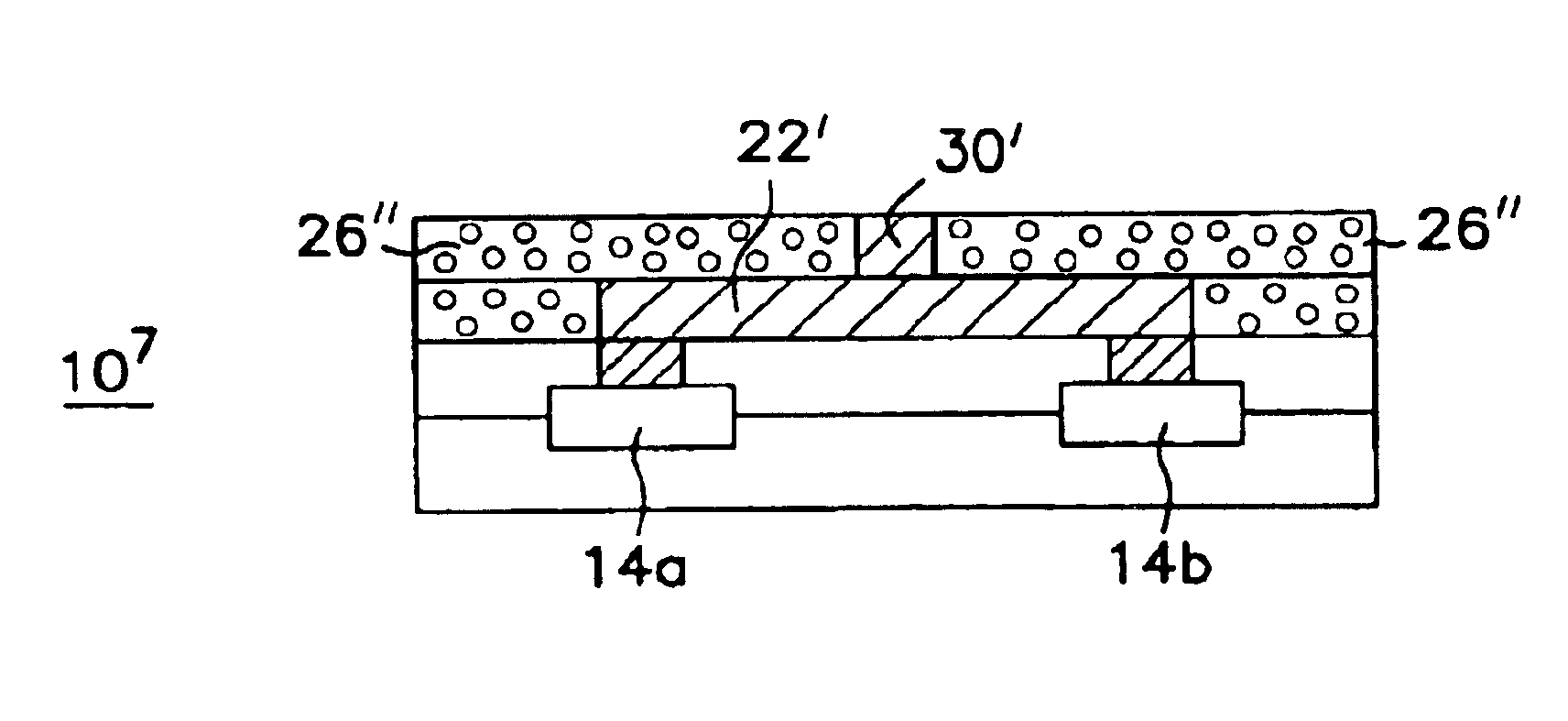
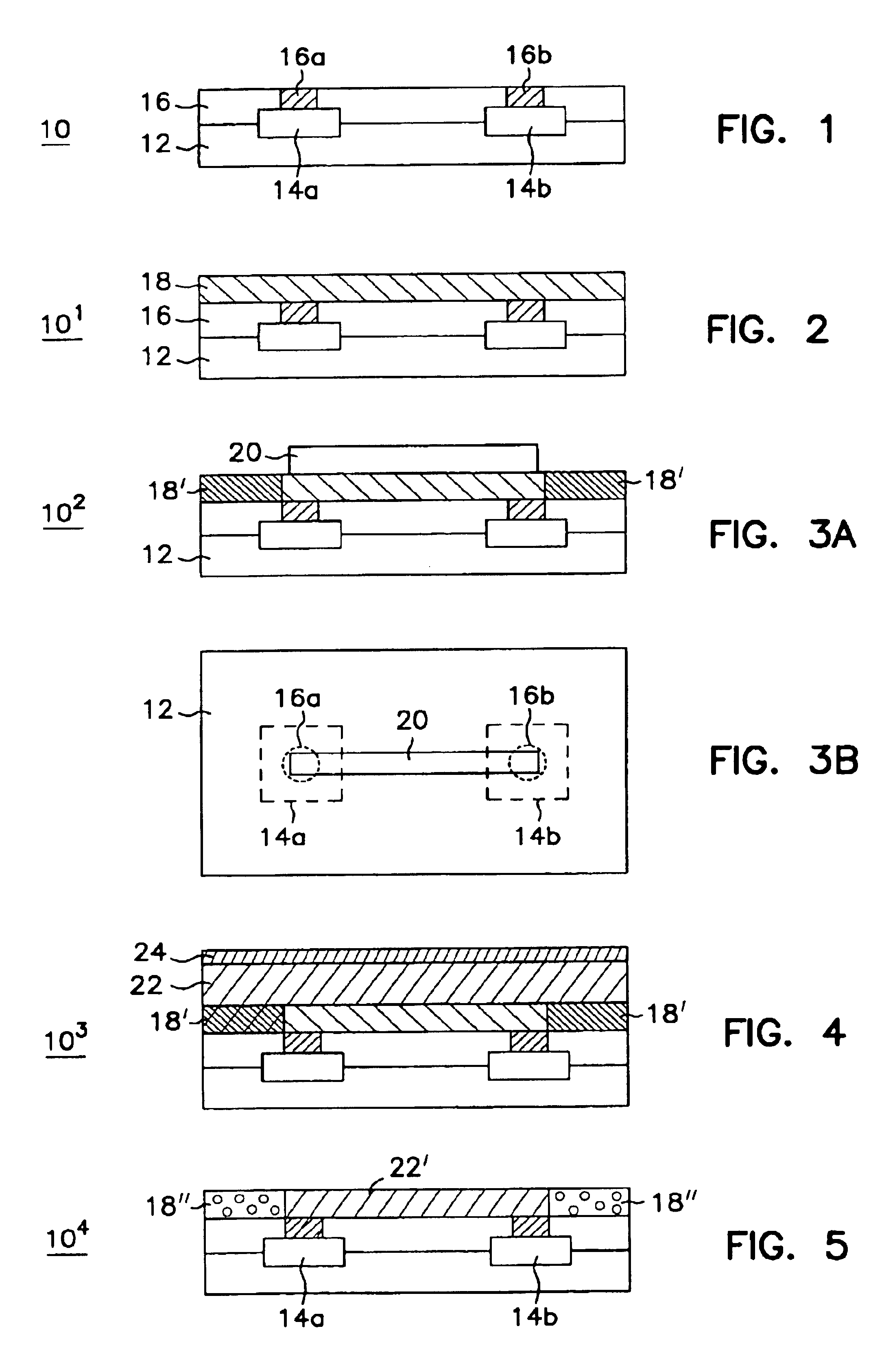
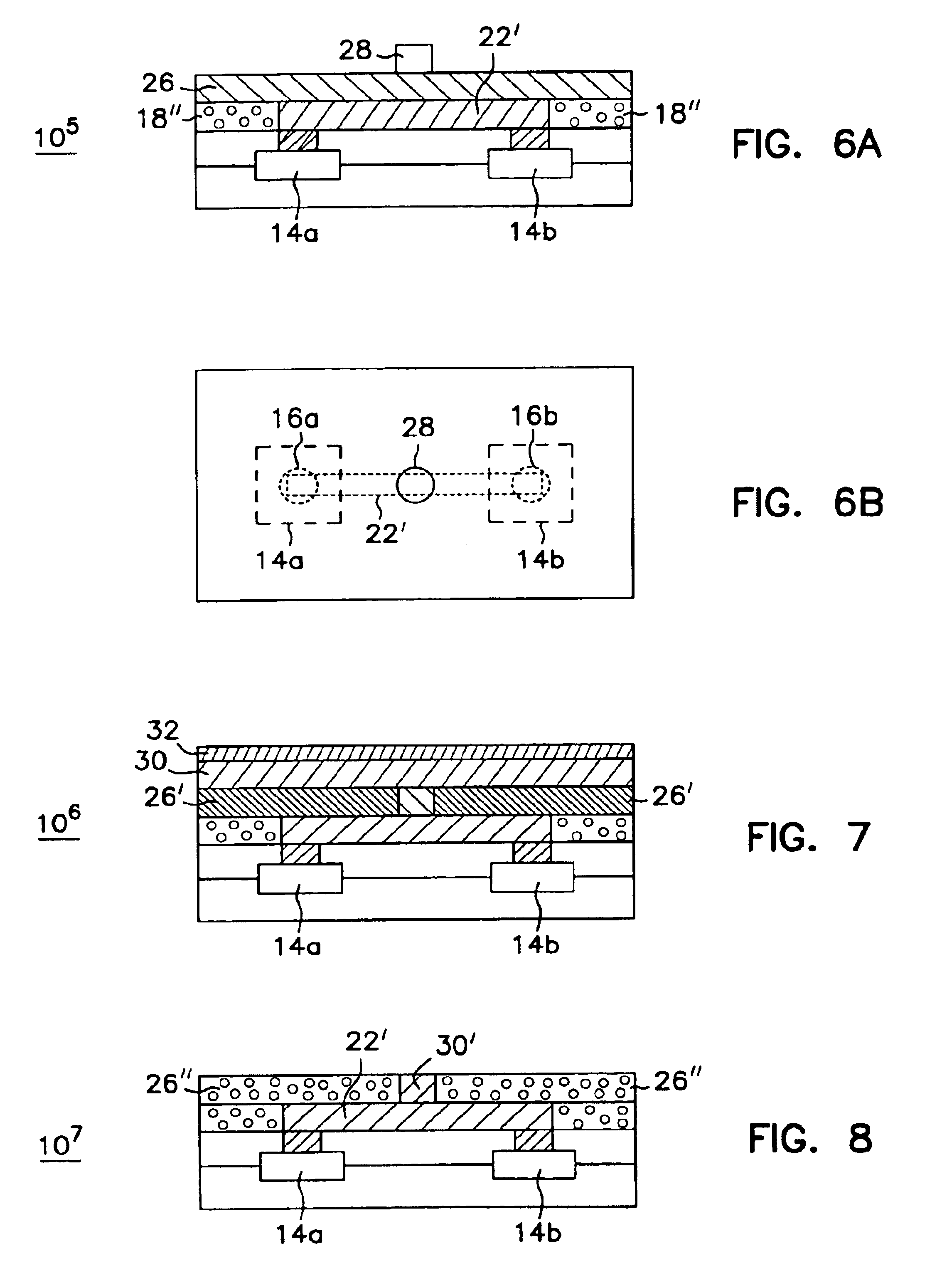
The following detailed description, which references and incorporates FIGS. 1-10, describes and illustrates specific embodiments of the invention. These embodiments, offered not to limit but only to exemplify and teach the invention, are shown and described in sufficient detail to enable those skilled in the art to practice the invention. Thus, where appropriate to avoid obscuring the invention, the description may omit certain information known to those of skill in the art.

The detailed description includes two sets of separate but overlapping embodiments of the invention. The first set of embodiments, illustrated principally with FIGS. 1-8, pertains to a preferred method of making single- and multi-level interconnective structures. The second set of embodiments, illustrated principally with FIGS. 9 and 10, concern hybrid interconnect structures which combine air bridges with structures exemplified in the first set of embodiments.

Preferred Method of Making Single- and Multi-Level In...


PUM


Abstract

A typical integrated-circuit fabrication requires interconnecting millions of microscopic transistors and resistors with metal wires. Making the metal wires flush, or coplanar, with underlying insulation requires digging trenches in the insulation, and then filling the trenches with metal to form the wires. The invention provides a new “trench-less” or “self-planarizing” method of making coplanar metal wires. Specifically, one embodiment forms a first layer that includes silicon and germanium; oxidizes a region of the first layer to define an oxidized region and a non-oxidized region; and reacts aluminum or an aluminum alloy with the non-oxidized region. The reaction substitutes, or replaces, the non-oxidized region with aluminum to form a metallic wire coplanar with the first layer. Another step removes germanium oxide from the oxidized region to form a porous insulation having a very low dielectric constant, thereby reducing capacitance.

Description

BACKGROUND OF THE INVENTIONThe present invention concerns methods of making, or fabricating, integrated circuits, particularly methods of forming interconnects.Integrated circuits, the key components in thousands of electronic and computer products, are interconnected networks of electrical components fabricated on a common foundation, or substrate. Fabricators typically use various techniques, such as layering, doping, masking, and etching, to build thousands and even millions of microscopic resistors, transistors, and other electrical components on a silicon substrate, known as a wafer. The components are then “wired,” or interconnected, together to define a specific electric circuit, such as a computer memory.Interconnecting millions of microscopic components typically entails covering the components with an insulative layer, etching small holes in the insulative layer to expose portions of the components underneath, and then actually connecting the components through metallizati...

Claims


Application Information

Patent Timeline
IPC IPC(8): H01L23/52H01L21/70H01L23/532H01L21/768
CPCH01L21/7682H01L21/76877H01L21/76886H01L23/53271H01L2924/0002Y10S438/933H01L2924/00H01L2221/1047
Inventor AHN, KIE Y.FORBES, LEONARDFARRAR, PAUL A.
Owner ROUND ROCK RES LLC
Why Eureka
Try Eureka