Semiconductor device with joint structure having lead-free solder layer over nickel layer

a technology of nickel layer and joint structure, which is applied in the direction of printed circuit assembling, conductive pattern reinforcement, printed circuit manufacture, etc., can solve the problems of user carelessness, adverse effect of pb (lead) on the environment, etc., and achieve the effect of low melting poin

Inactive Publication Date: 2005-04-12
RENESAS ELECTRONICS CORP
View PDF5 Cites 87 Cited by
  • Summary
  • Abstract
  • Description
  • Claims
  • Application Information

AI Technical Summary

Benefits of technology

In recent years, an adverse effect of Pb (lead) on the environment has been regarded as a problem. Thus, in semiconductor devices, technique for making Pb free has been actively investigated. In BGA type semiconductor devices, as a terminal for external connect, there is generally used a solder bump having a Pb—Sn (tin) eutectic composition (63[wt %]Pb—37[wt %]Sn) having a low melting point. At present, however, Pb-free solder bumps, for example, solder bumps having composition of a Sn—Ag (silver) —Cu (copper) are being used.

Problems solved by technology

In recent years, an adverse effect of Pb (lead) on the environment has been regarded as a problem.
In particular, portable electronic instruments such as a portable telephone are exposed to danger of falling by user's carelessness.

Method used


Image

  • Semiconductor device with joint structure having lead-free solder layer over nickel layer
  • Semiconductor device with joint structure having lead-free solder layer over nickel layer
  • Semiconductor device with joint structure having lead-free solder layer over nickel layer

Examples


embodiment 1

In the present embodiment 1, examples wherein the present invention is applied to a BGA type semiconductor device having a wire bonding structure and a module into which the device is integrated will be described.

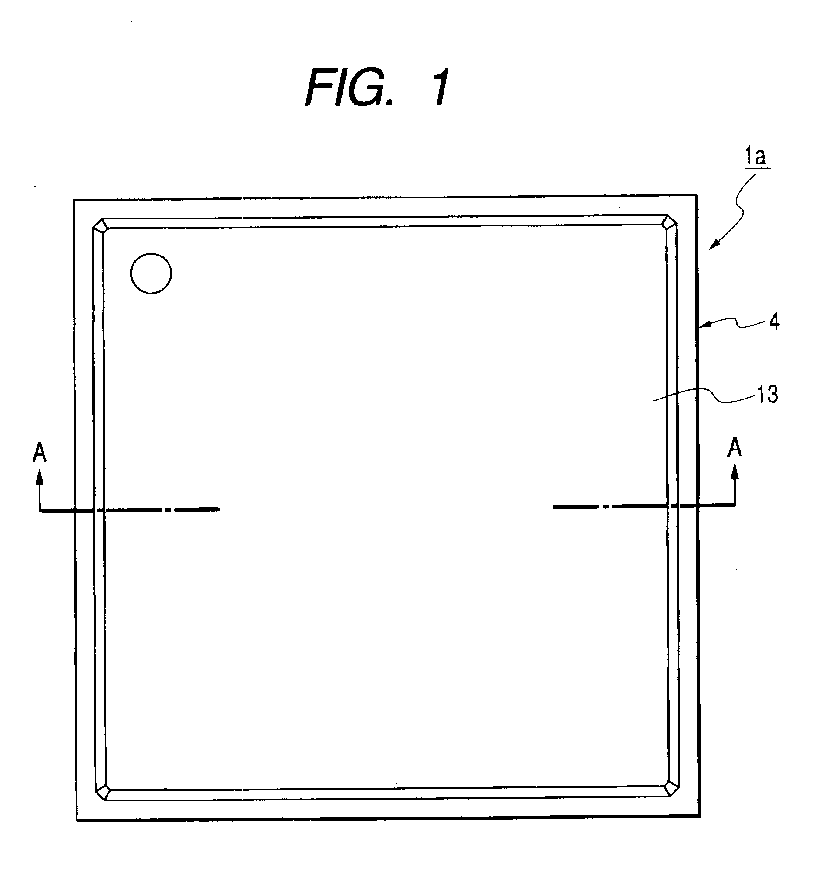
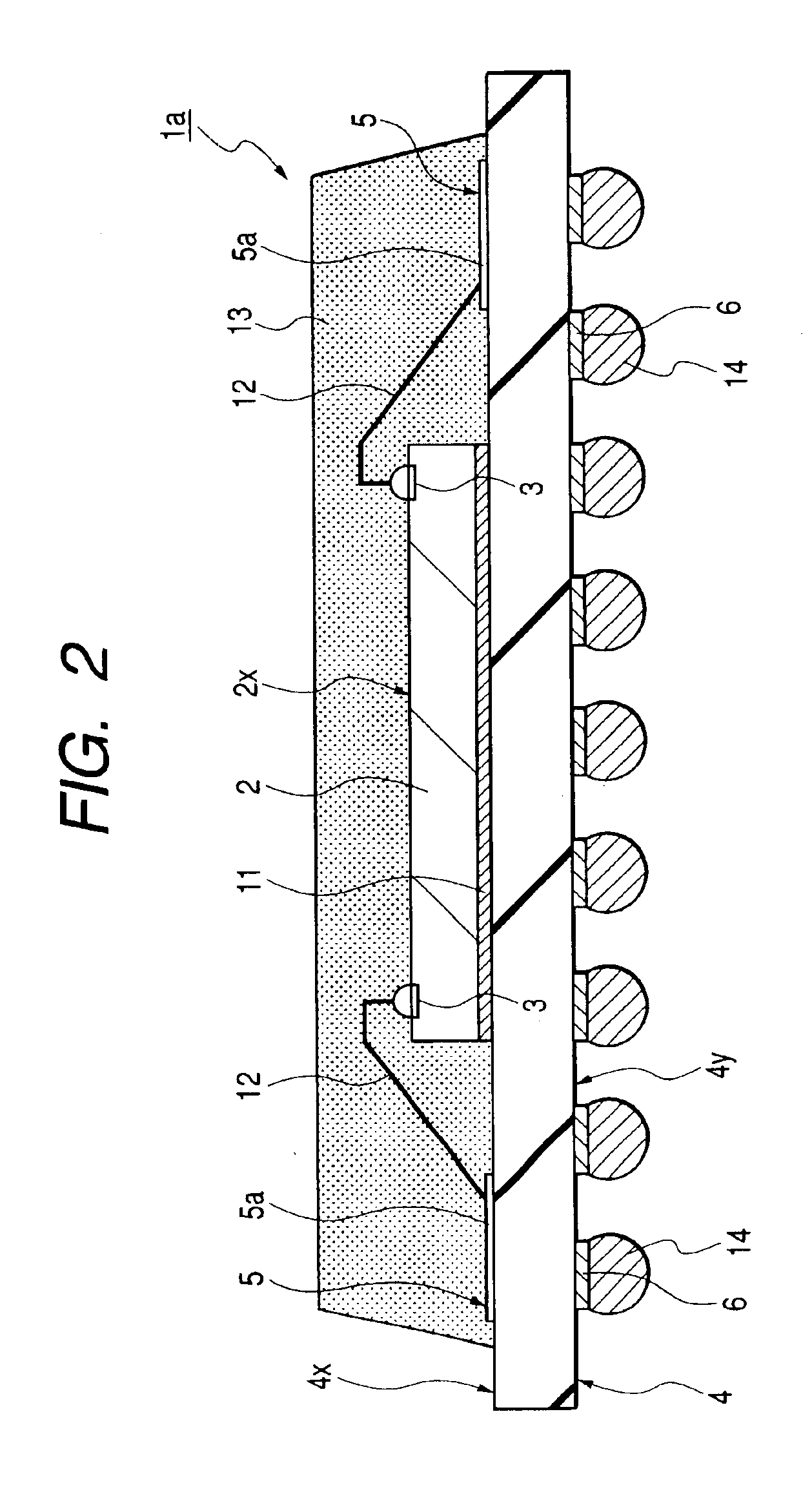
FIG. 1 is a plan view illustrating an outline of the BGA type semiconductor device, which is according to the embodiment 1 of the present invention, FIG. 2 is a sectional view taken along A—A line of FIG. 1, FIG. 3 is a partially enlarged sectional view of FIG. 2, FIG. 4 is a partially enlarged sectional view of FIG. 3, FIGS. 5(a) and 5(b) are views illustrating an outline of an interposer (wiring board) used in the manufacture of the BGA type semiconductor device according to the embodiment 1 of the present invention (FIG. 5(a) is a bottom view thereof, and FIG. 5(b) is a sectional view thereof). FIGS. 6(a) to 6(d) are views for explaining the manufacture of the semiconductor device according to the embodiment 1 of the present invention (FIGS. 6(a) to 6(d) are sectional vi...

embodiment 2

In the present embodiment 2, an example wherein the present invention is applied to an LGA type semiconductor device will be described.

FIG. 29 is a sectional view illustrating an outline of a semiconductor device according to the present embodiment 2, and FIG. 30 is a partially enlarged sectional view of FIG. 29.

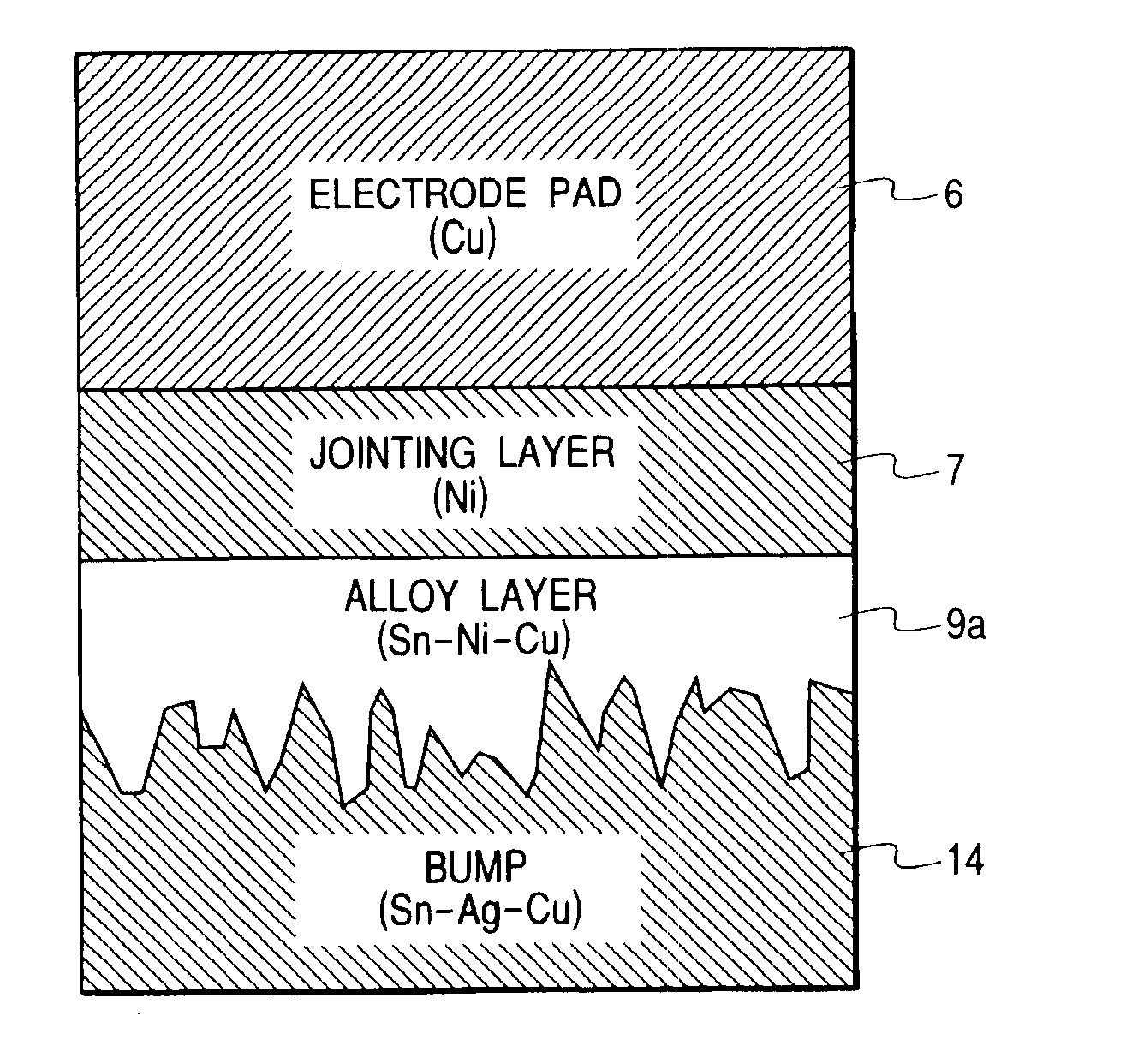
As illustrated in FIG. 29, the LGA type semiconductor device 1b has a structure wherein a semiconductor chip 2 is mounted on the side of a main face 4x of an interposer 4 and plural electrode pads 6 are arranged, as terminals for external connection, on the side of a rear face 4y of the interposer 4.

As illustrated in FIG. 30, a jointing layer 7 made of a Ni plating layer is deposited on the surfaces of the electrode pads 6, and a Au film 8 made of, for example, a plating layer is deposited as an antioxidation film on the surface of the jointing layer 7.

The LGA type semiconductor device 1b is mounted on a mount board with a solder layer being interposed between the electrode ...

embodiment 3

In the present embodiment 3, an example wherein the present invention is applied to a BGA type semiconductor device having a face down bonding structure will be described.

FIG. 31 is a sectional view illustrating an outline of a BGA type semiconductor device according to the embodiment 3 of the present invention, and FIG. 32 is a partially enlarged sectional view of FIG. 31.

As illustrated in FIG. 31, the BGA type semiconductor device 1c has a structure wherein a semiconductor chip 60 is mounted on the side of a main face 64x of an interposer 64 and plural solder bumps 14 are arranged, as terminals for external connection, on the side of a rear face 64y of the interposer 64.

Plural electrode pads 62 are formed on a main face 60x of the semiconductor chip 60. Plural electrode pads 65 are formed on the main face 64x of the interposer 64, correspondingly to the electrode pads 62 of the semiconductor chip 64, and plural electrode pads 6 are formed on the rear face 64y of the interposer 64....


PUM

PropertyMeasurementUnit
thicknessaaaaaaaaaa
diameteraaaaaaaaaa
diameteraaaaaaaaaa

Abstract

The impact strength resistance of a solder joint portion of a semiconductor device is improved. The semiconductor device has a joint structure wherein a jointing layer which does not contain sulfur substantially is arranged between an underlying conductive layer and a lead-free solder layer and further between the jointing layer and the lead-free solder layer is formed an alloy layer comprising elements of these layers.

Description

BACKGROUND OF THE INVENTIONThe present invention relates to a semiconductor device, a method of manufacturing the same, an electronic instrument, and a technique of manufacturing the same, in particular, a semiconductor device integrated into a portable instrument, and a technique which is effectively applied to an electronic instrument.As a semiconductor device, for example, a semiconductor device called BGA (ball grid array) type device is known. This BGA type semiconductor device has a package structure wherein semiconductor chips are mounted on the side of the main face of a wiring board called interposer and plural solder bumps are arranged, as terminals for external connection, on the rear face side which is opposite to the main face of the wiring board.BGA type semiconductor devices having various structures have been developed and made practicable as manufactured goods. The structures of the BGA type semiconductor devices are roughly classified into wire bonding structures a...

Claims


Application Information

Patent Timeline
Patent Type & Authority Patents(United States)
IPC IPC(8): H01L23/498H01L23/485H01L23/48H05K3/24H05K3/34H01L23/12H01L21/60
CPCH01L23/49816H01L24/10H05K3/244H01L24/13H01L2224/13099H01L2224/16225H01L2224/32225H01L2224/48095H01L2224/48227H01L2224/48465H01L2224/73204H01L2224/73265H01L2224/92247H01L2924/01004H01L2924/01011H01L2924/01013H01L2924/01015H01L2924/01016H01L2924/01029H01L2924/01078H01L2924/01079H01L2924/01082H01L2924/01322H01L2924/01327H01L2924/14H01L2924/15311H05K3/3463H01L2924/0133H01L24/48H01L2924/01005H01L2924/01006H01L2924/01033H01L2924/01047H01L2924/01055H01L2924/014H01L2924/013H01L2224/45144H01L2924/00014H01L2924/00H01L2924/00012H01L24/03H01L24/05H01L24/16H01L24/45H01L24/73H01L2224/02377H01L2224/05001H01L2224/05008H01L2224/05022H01L2224/05024H01L2224/05027H01L2224/05568H01L2224/05569H01L2224/05572H01L2224/05573H01L2224/13H01L2924/181H01L2224/05541H01L2224/05005H01L23/48
Inventor YAMAMOTO, KENICHIMORITA, TOSHIAKIYAMADA, MUNEHIROKIMOTO, RYOSUKE
Owner RENESAS ELECTRONICS CORP
Why Eureka
Try Eureka