Method to detect systematic defects in VLSI manufacturing

a technology of vlsi chip manufacturing and systematic defects, applied in the direction of individual semiconductor device testing, semiconductor/solid-state device testing/measurement, instruments, etc., can solve the problems of almost impossible to achieve perfect yields in vlsi chip manufacturing and assumed manufacturing defects

Inactive Publication Date: 2005-04-12
GLOBALFOUNDRIES INC
View PDF11 Cites 30 Cited by
  • Summary
  • Abstract
  • Description
  • Claims
  • Application Information

AI Technical Summary

Benefits of technology

VLSI manufacturing yield enhancement involves detecting root causes of defects. The present invention is directed to a method using software based analysis of fail data and d...

Problems solved by technology

Manufacturing defects are assumed when the results do not match what is expected.
Assuming the scan chains are faultless, the defect is located in the sub-circuit involved in computing the unexpected logic values.
Perfect yields in VLSI chip manufacturi...

Method used


Image

  • Method to detect systematic defects in VLSI manufacturing
  • Method to detect systematic defects in VLSI manufacturing
  • Method to detect systematic defects in VLSI manufacturing

Examples


Embodiment Construction

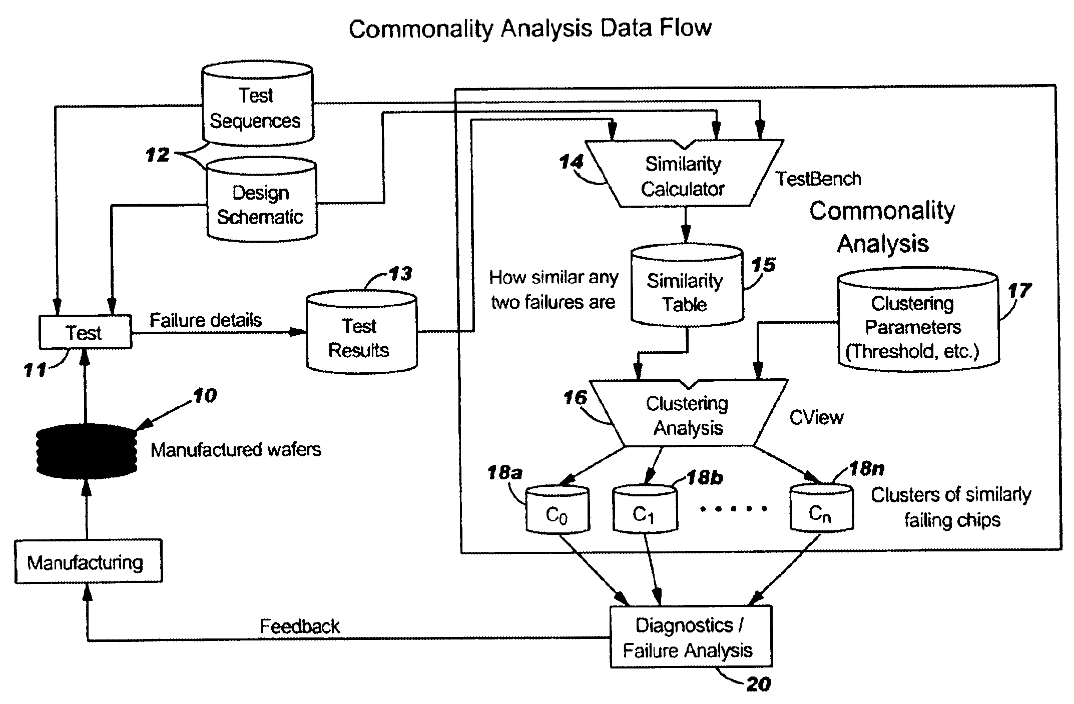
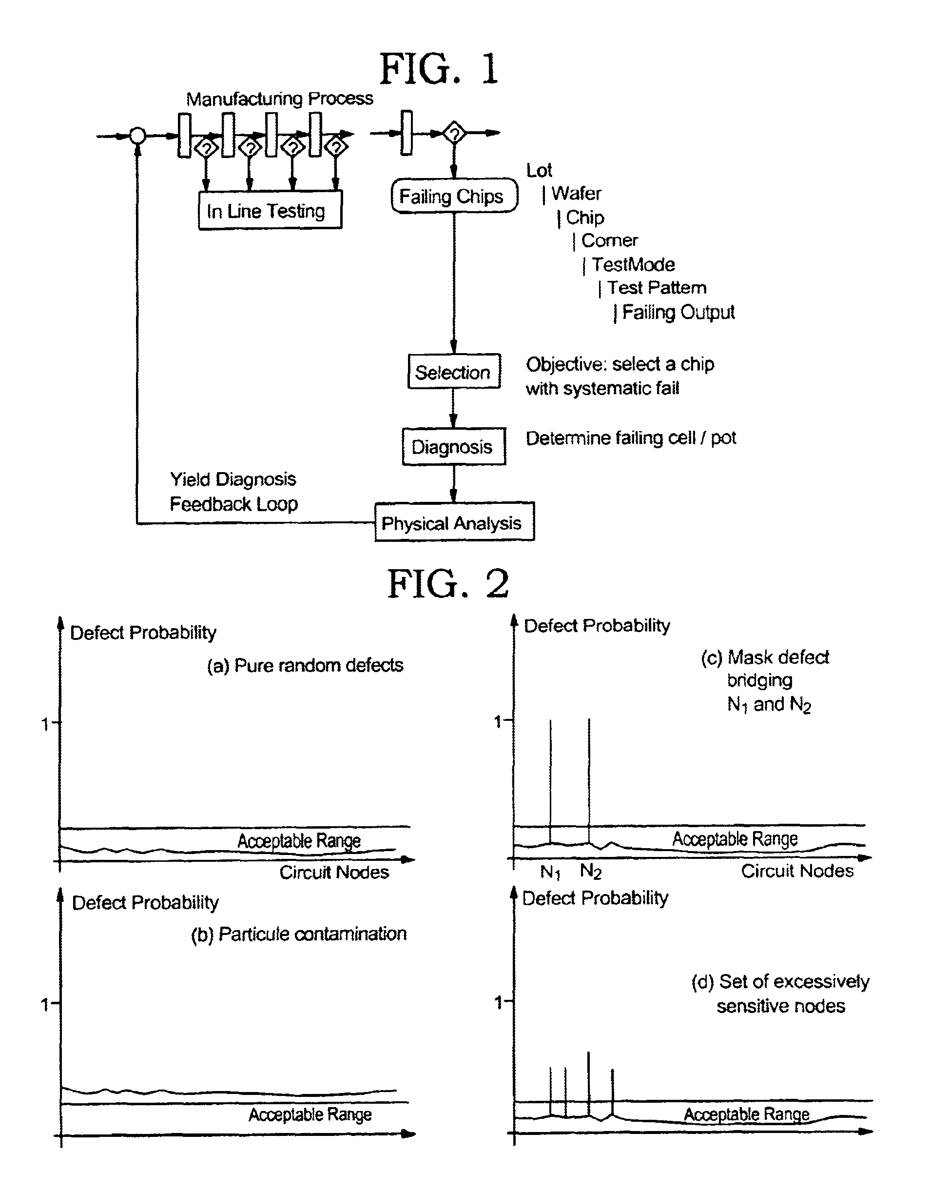
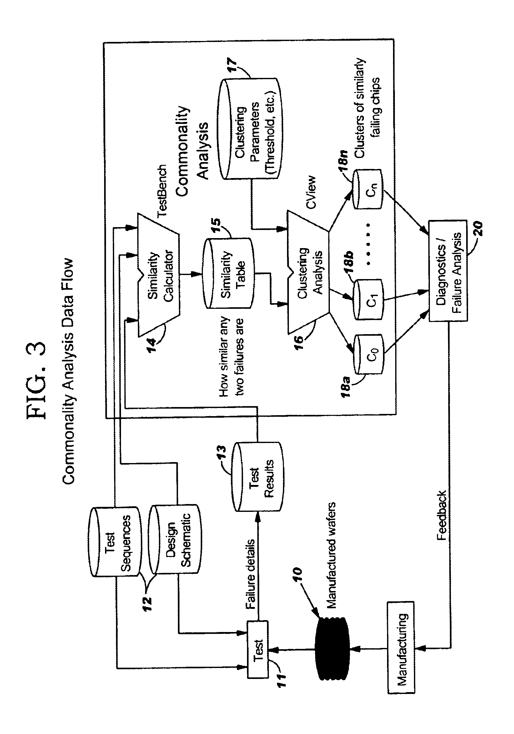
Attention is now directed to FIG. 3, which illustrates the data flow and how the commonality analysis is performed in accordance with the present invention. After the wafers 10 are manufactured, various tests 11 are performed using LSSD, scan chains using applicable test sequences 12, and the logic design description. The test result 13 are collected and transmitted to the similarity calculator 14, along with the applicable test sequences 12 and the logic design description. The results of the similarity calculator are transmitted to similarity table 15. Table 15 is fed into the clustering analysis 16, along with certain clustering parameters 17. The results of the clustering analysis determines the clusters of similarly failing chips 18a. . . 18n. These results may be used in diagnostics and failure analysis 20, and be fed back to improve manufacturing of the wafers.

We will now focus on the simularity calculator 14. During testing it is necessary to track the latches that contain i...


PUM


Abstract

Defects in manufacturing of IC devices are analyzed by testing the devices for defects using results of LSSD technology to find at least one failing pattern that contains incorrect values. The failing latches are used as a starting point to trace back through combinational logic feeding the failing latches, until controllable latches are encountered. A decision is then made to continue the back tracing or not depending on whether the latter latches were clocked during the application of one of the failing patterns or not.

Description

FIELD OF THE INVENTIONThis invention relates to the analysis of defects detected in integrated circuit (IC) devices manufactured using VLSI technology. More particularly, the invention is directed to detecting structural commonalities of VLSI manufacturing defects.BACKGROUNDWith modem manufacturing techniques, the yield of digital CMOS or memory circuits is primarily limited by random defects that result from random effects such as dust particles or other materials floating in the air, a person coughing or sneezing, etc. Non-random (systematic) defects that result from problems with the manufacturing process and are reproduced regularly on successive ICs, as well as parametric defects in which a part may not quite meet specifications but is still functional, should be reduced or eliminated through rapid learning techniques during the course of manufacturing products in large volumes.IC chips are fabricated as separate dies on semiconductor wafers. Each die is probed for testing, wit...

Claims


Application Information

Patent Timeline
IPC IPC(8): H01L21/66
CPCH01L22/20H01L2924/0002H01L2924/00
Inventor HUISMAN, LEENDERT M.KASSAB, MAROUNPASTEL, LEAH M. P.
Owner GLOBALFOUNDRIES INC
Why Eureka
Try Eureka