Method of processing selected surfaces in a semiconductor process chamber based on a temperature differential between surfaces

a technology of semiconductor process chamber and temperature differential, which is applied in the direction of cleaning hollow objects, lighting and heating apparatus, and using liquids to clean objects, etc., can solve the problems of rtp system certain disadvantages that have not been adequately addressed, defective devices being formed on wafers, and prolonged heating and cooling of wafers

Inactive Publication Date: 2005-04-19
MICRON TECH INC
View PDF4 Cites 14 Cited by
  • Summary
  • Abstract
  • Description
  • Claims
  • Application Information

AI Technical Summary

Benefits of technology

[0014]The present invention overcomes the disadvantages of the prior art by providing a method by which a reactant may favor a reaction with selected surfaces in a semiconduct

Problems solved by technology

Unnecessary heating may lead to defective devices being formed on the wafer.
Thus, in hot wall process chambers a wafer may be subject to prolonged heating and cooling.
However, RTP systems have certain disadvantages that have not been adequately addressed.
One significant disadvantage is that radiant energy may not be absorbed uniformly by a wafer.
This results in temperature variations in and across the wafer.
Temperature variations lead to non-uniform process results.
Unfortunately, a significant disadvantage of this temperature monitoring system is its vulnerability to certain cleaning processes carried out in an RTP process chamber.
Poor, irregular HSG formations result in unclean RTCVD process chambers.
An undesired side effect from polysilicon deposition is that the polysilicon is deposited not only on the wafer but also on other surfaces in the process chamber.
A build-up of polysilicon impedes the transmission of radiant energy through the window onto the wafer.
It may also lead to high particle counts in the chamber, lowering production yields.
The '195 patent does no

Method used


Image

  • Method of processing selected surfaces in a semiconductor process chamber based on a temperature differential between surfaces
  • Method of processing selected surfaces in a semiconductor process chamber based on a temperature differential between surfaces
  • Method of processing selected surfaces in a semiconductor process chamber based on a temperature differential between surfaces

Examples


example embodiment

OF THE INVENTION

Cycled in Situ Clean of an RTCVD Process Chamber Using NF3 Gas

[0063]The following is one example embodiment of the invention, which was tested by the inventor. The example is intended to help illustrate and further describe the foregoing principles of the invention. The information in the example embodiment is believed to be reasonably complete and accurate. Notwithstanding the inclusion of this example, the inventor believes the patentability of the present invention has been established independently of this example by the foregoing description and attached figures.

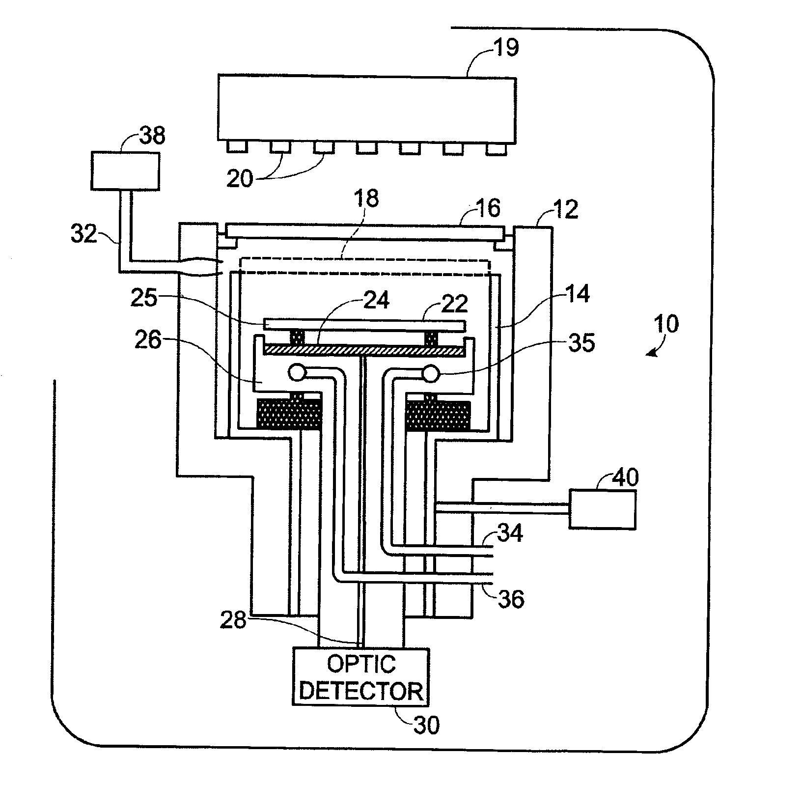
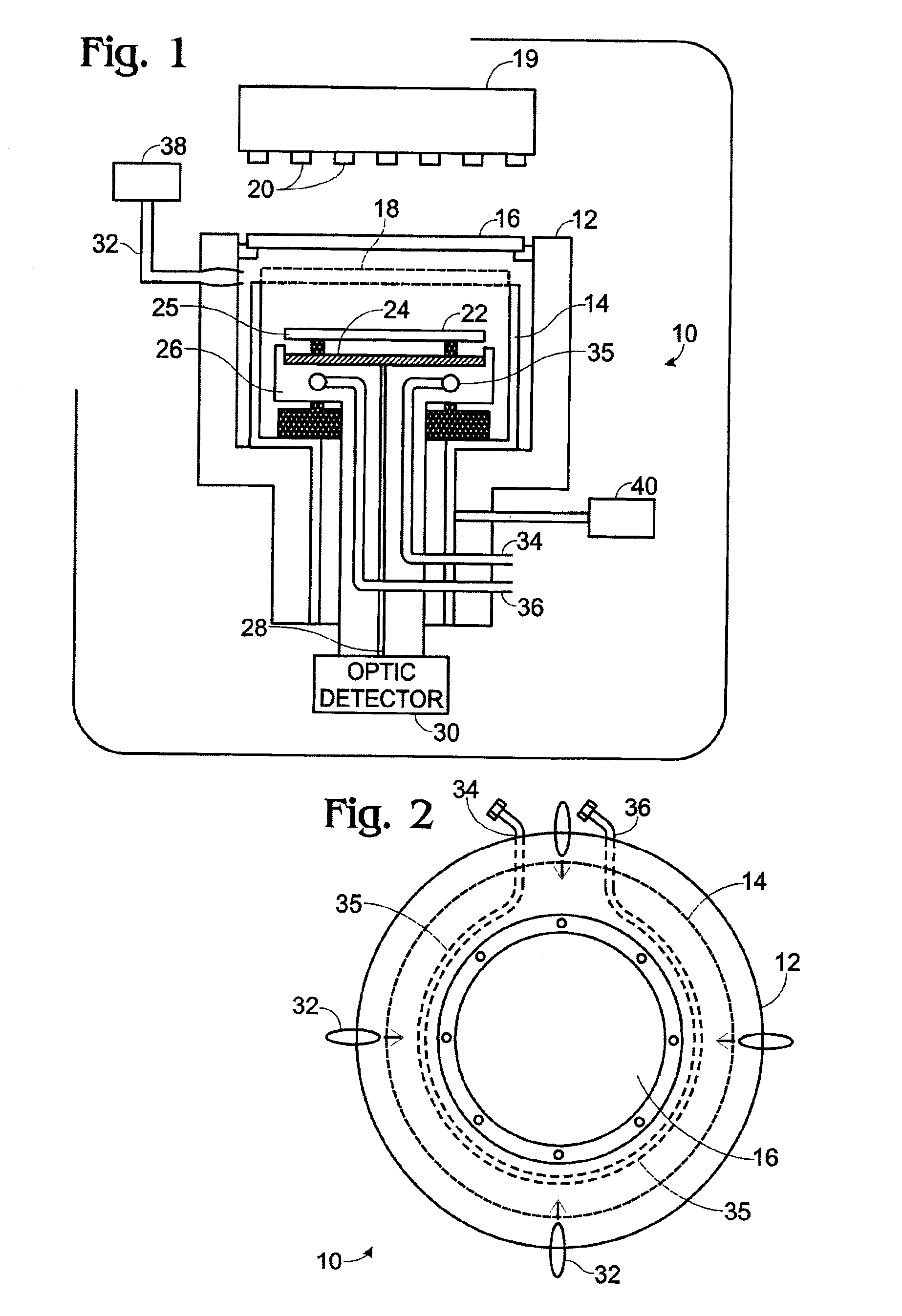
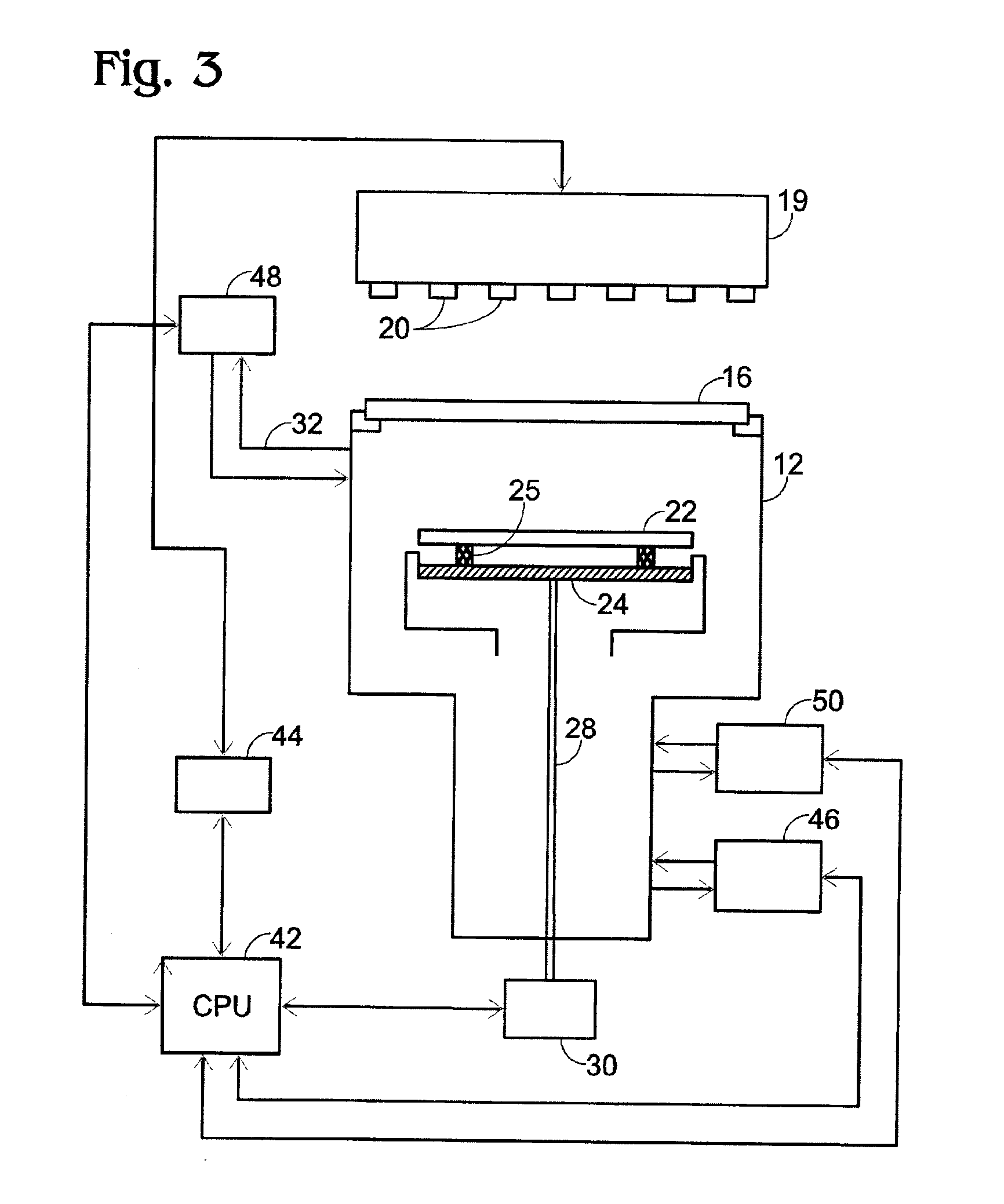
[0064]The following testing was carried out to determine if NF3 gas could be used to clean an AGI Integra Pro clustered RTCVD process chamber of polysilicon deposits. The Integra Pro is manufactured by AG Associate Israel. The test evaluated whether the cleaning process would cause damage to the temperature measurement system or other components of the process chamber. The test also evaluated the impact ...


PUM

PropertyMeasurementUnit
Temperatureaaaaaaaaaa

Abstract

The present invention relates to a method of processing selected surfaces in a semiconductor process chamber by creating a temperature differential between the selected surfaces and contacting the surfaces with a reactant that preferentially react with a surface at one end of the temperature differential relative to the other selected surface(s). More particularly, the invention relates to the use of nitrogen trifluoride (NF3) gas for in situ cleaning of cold wall process chambers such as Rapid thermal Chemical Vaporization (“RTCVD”) systems.

Description

[0001]This application is a divisional of U.S. patent application Ser. No. 09 / 246,611, filed Feb. 8, 1999 now U.S. Pat. No. 6,395,099. The priority of the prior application is expressly claimed and its disclosure is hereby incorporated by reference in its entirety.BACKGROUND OF THE INVENTION[0002]The present invention relates to a method of processing a selected surface in a semiconductor process chamber by contacting the selected surface with a reactant that reacts preferentially with the selected surface relative to another surface when the selected surface is at a different temperature from the other surface. The invention is particularly suited for use in rapid thermal processing (RTP) systems. More particularly, the invention relates to the use of nitrogen trifluoride (“NF3”) gas to clean selected surfaces in RTP process chambers, including in Rapid Thermal Chemical Vapor Deposition (RTCVD) process chambers.[0003]During the course of semiconductor device fabrication, a wafer un...

Claims


Application Information

Patent Timeline
IPC IPC(8): C23C16/44
CPCC23C16/4405Y10S438/905
Inventor PAN, JAMES
Owner MICRON TECH INC
Why Eureka
Try Eureka