Semiconductor die adapter and method of using

a technology of silicon die and adapter, which is applied in the direction of individual semiconductor device testing, semiconductor/solid-state device testing/measurement, instruments, etc., can solve the problems of low yield of functioning mcm's, low efficiency of mcm's, and high percentage of chips on a wafer that function properly, etc., to achieve less damage, greater surface area, and more robust

Inactive Publication Date: 2005-04-19
THE JOHN HOPKINS UNIV SCHOOL OF MEDICINE
View PDF14 Cites 7 Cited by
  • Summary
  • Abstract
  • Description
  • Claims
  • Application Information

AI Technical Summary

Benefits of technology

[0011]The present invention is directed to a semiconductor die adapter assembly. An object of the present invention is to provide a second set of bond pads on the die adapter so that electrical connections to the original bond pads on the die are not broken and remade during bum-in testing of a die. Another object of the present invention is to provide bond pads on a semiconductor die adapter that are more robust than the relatively fragile bond pads on the die. Yet another object of the present invention is to provide a durable semiconductor die adapter that is less subject to damage caused by die handling tools than a bare semiconductor die. Still another object of the present invention is to provide a semiconductor die adapter that has bond pads of greater surface area than the bond pads of its associated die to enable easier electronic testing of the die.

Problems solved by technology

However, because the yield of a wafer (i.e., the percentage of chips on a wafer that function properly) is often not very high, it is important to determine which chips are defective and which chips are functional before the chips are packaged.
Otherwise, the compound effect of the individual yields of the different chips can result in very low yields of functioning MCM's.
Defective dice are generally expected to fail after a certain number of hours of burn-in testing.
Sometimes it is not feasible to conduct a final die test before dice are cut from a wafer.
Such final testing procedures can be difficult and time consuming and particular care must be taken so that the testing procedure itself doesn't damage an otherwise good die.
These procedures have several inherent problems.
First, to be successfully tested in a temporary package, a die often requires enlarged pads, to which the test leads of the package are wire bonded, and the enlarged pads can reduce integrated circuit density.
Dies with a small pad pitch, i.e., center-to-center distance between the pads, make it difficult to reliably connect test leads.
Second, the bond wires of the test package often need to be broken off and removed from the chips before final packaging.
The process of removing bond wires will frequently damage the bond pads of a die.
Finally, the above procedures require an excessive amount of die handling that increases the chances of damaging the die.

Method used


Image

  • Semiconductor die adapter and method of using
  • Semiconductor die adapter and method of using
  • Semiconductor die adapter and method of using

Examples


first embodiment

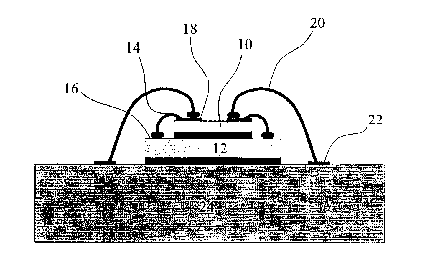
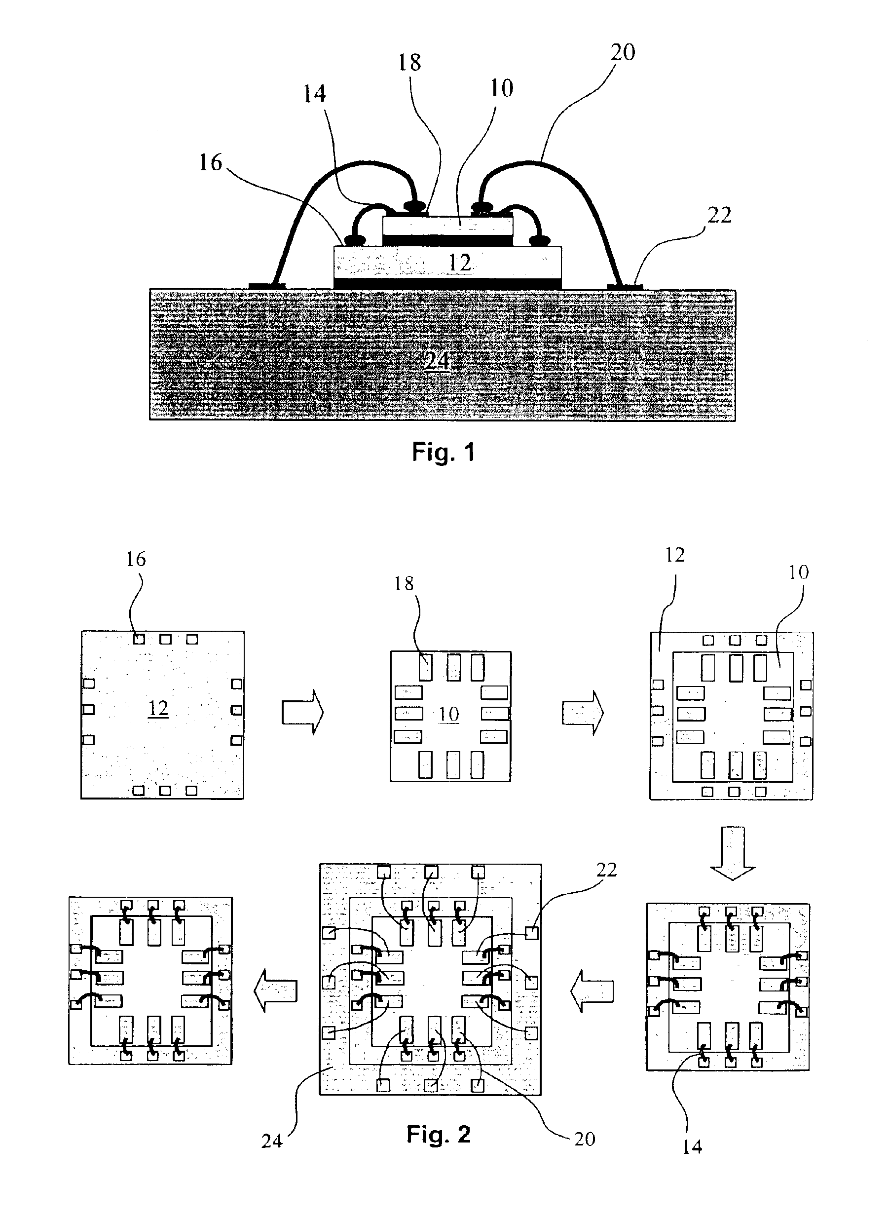
[0020]the present invention is illustrated in FIG. 1. It includes an adapter 10 that is bonded to the active side of an integrated circuit die 12. Die-to-adapter connectors 14 connect die bond pads 16 to corresponding adapter bond pads 18. Finally, adapter-to-substrate connectors 20 connect the adapter bond pads 18 to device contacts 22 on a device substrate 24 such as a printed circuit board or module.

[0021]A significant feature of the present invention teaches that the adapter 10 may be permanently bonded to the die 12 so that the adapter 10 may accompany the die 12 through testing in a temporary package and into final assembly in a device or module. That means that the die-to-adapter connectors 14 are bonded to the die bond pads 16 only once. The adapter bond pads 18 may be designed to be larger and more robust than the corresponding die bond pads 16. Increasing bond pad surface area on the adapter 10 results in more reliable bonds. Also, because connections to the relatively fra...

second embodiment

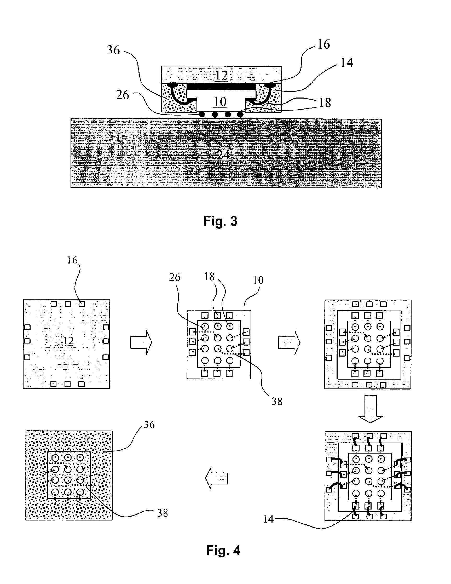
[0027]FIG. 3 illustrates the present invention involving a flip chip. Here the adapter 10 and the die 12 are turned upside down and the active surface of the die 12 faces the substrate. The die-to-adapter connectors 14 may again comprise wire bonds; however the adapter-to-substrate connectors 20 may comprise, instead of wire bonds, reflowed solder bumps 26 connected to the underside of the adapter 10. The solder bumps 26, another source of frequent defects and shorts in traditional integrated circuit packages, are attached to the more robust adapter bond pads 18. A polymer encapsulant 36 may be added around the base of the die 12 to protect the electrical connections.

[0028]FIG. 4 is a process flow diagram illustrating bottom views of the embodiment shown in FIG. 3 during various stages of fabrication. Starting with a bare flip chip die 12 shown in the upper left hand corner of FIG. 4, the adapter 10 is bonded to the die 12 and wire bonds are used as the die to adapter electrical con...


PUM


Abstract

A semiconductor die adapter assembly includes a semiconductor die cut from a wafer, the die having an active surface including bond pads. A die adapter, also having bond pads, is bonded to the semiconductor die. Die-to-adapter connectors electrically connect the die bond pads to the adapter bond pads. Finally, adapter-to-substrate connectors electrically connect the adapter bond pads to a device substrate. Having bond pads on the die adapter eliminates the need to break and remake the electrical connections to the original bond pads on the die during burn-in testing of the die.

Description

CROSS-REFERENCE TO RELATED APPLICATION[0001]This application claims the benefit of the co-pending U.S. Provisional Application No. 60 / 294,737, filed on May 31, 2001.BACKGROUND OF THE INVENTION[0002]1. Field of the Invention[0003]The present invention relates to an apparatus and method for reliably testing and installing individual integrated circuit chips using die adapters that minimize damage to the chips.[0004]2. Description of the Related Art[0005]A semiconductor die (plural “dice”) is an integrated circuit designed to serve a specific function, such as a memory chip, in an electronic device. Dice are generally fabricated together in rows on a silicon wafer. During die fabrication, also known as wafer processing, photolithography is traditionally used to first print an image of the micro-circuitry of each die on a wafer surface, duplicating the circuit image at each adjacent die location until the wafer surface is filled. Subsequent processing often including ion implantation, e...

Claims


Application Information

Patent Timeline
Patent Type & Authority Patents(United States)
IPC IPC(8): G01R1/02G01R1/04H01L23/498H01L23/48G01R31/28
CPCG01R1/0416H01L23/49827G01R31/2884H01L2924/07811H01L2924/10253H01L2924/19107H01L2224/32145H01L2224/48471H01L2924/01079H01L2924/14H01L24/48H01L2224/73215H01L2224/73265H01L2924/00H01L2224/05624H01L2224/05644H01L2924/181H01L2224/45099H01L2224/85399H01L2924/00014H01L2224/4826H01L2224/48464H01L2224/49109H01L24/49H01L2924/00012H01L2224/45015H01L2924/207
Inventor LE, BINH Q.LEW, ARK L.CHARLES, JR., HARRY K.SCHWARTZ, PAUL D.LEHTONEN, SEPPO J.LING, SHARON X.
Owner THE JOHN HOPKINS UNIV SCHOOL OF MEDICINE
Why Eureka
Try Eureka