On-system programmable and off-system programmable chip
a programmable chip and on-system technology, applied in the field of programmable chips, can solve the problems of large chip area, high cost, and inability to employ a pumping circuit in each chip, and achieve the effect of reducing the cost of manufacturing, increasing the chip area and manufacturing cost, and increasing the cost of manufacturing
- Summary
- Abstract
- Description
- Claims
- Application Information
AI Technical Summary
Benefits of technology
Problems solved by technology
Method used
Image
Examples
first embodiment
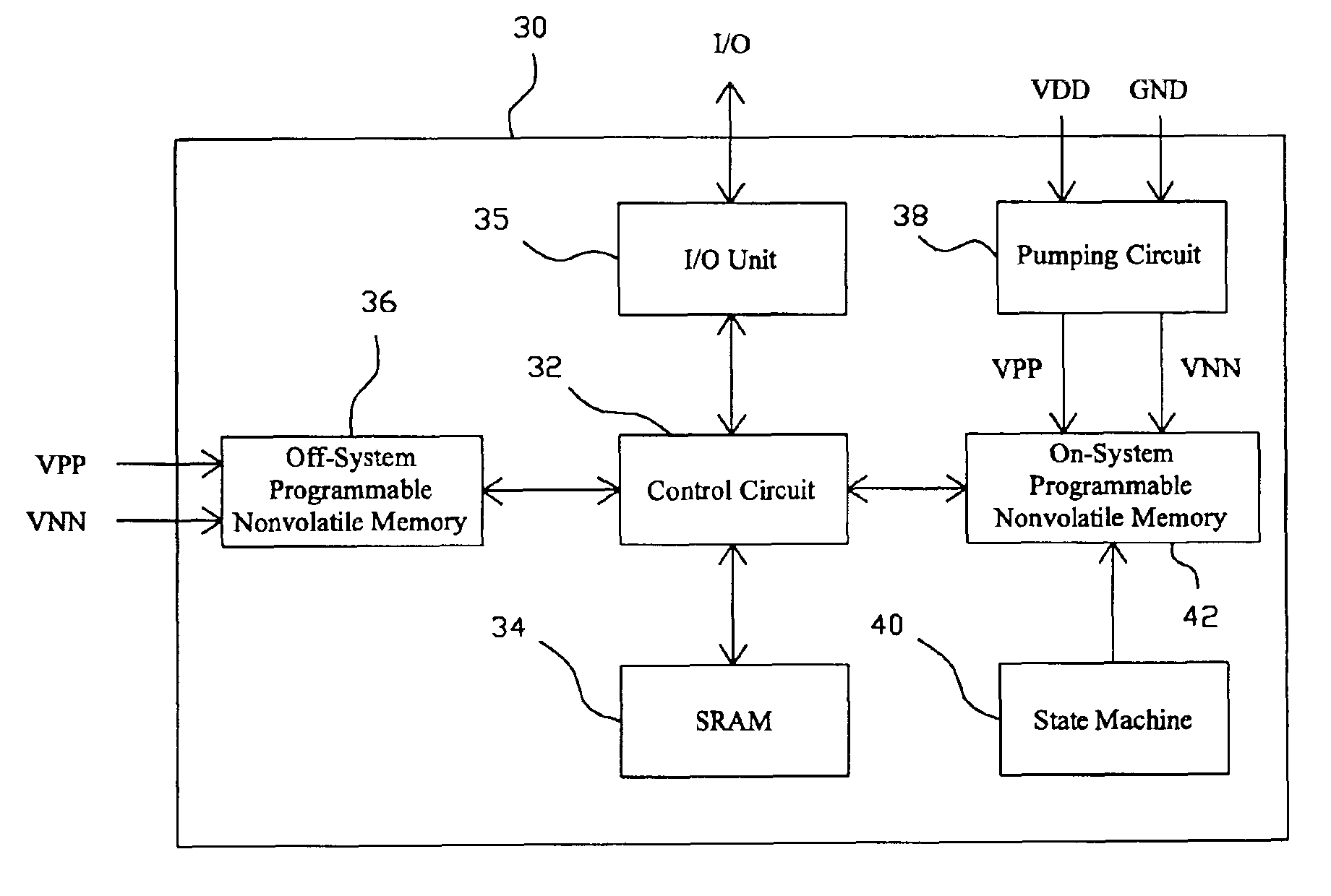
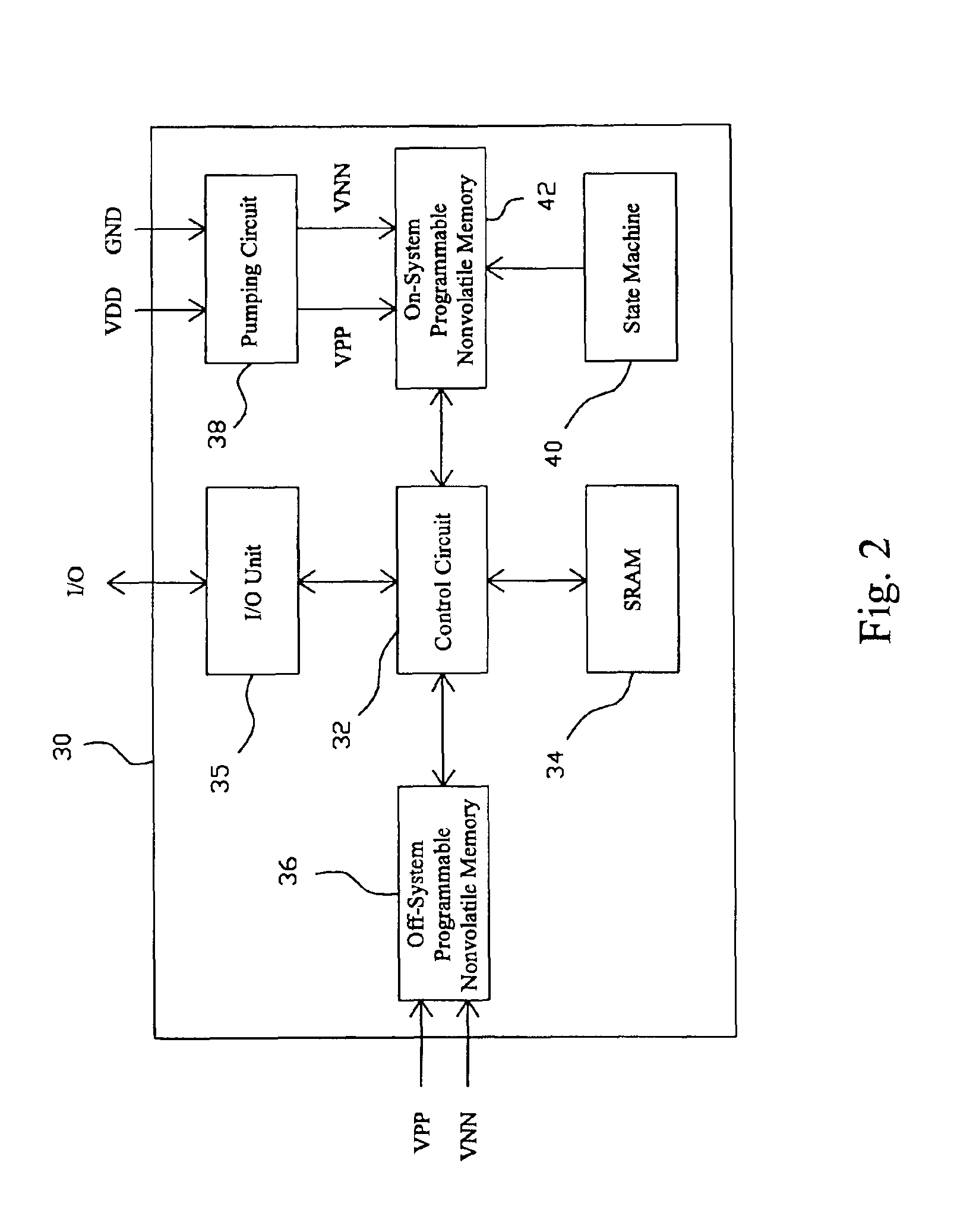
[0017]FIG. 2 is a diagram of the first embodiment according to the present invention. In chip 30, a control circuit 32 is connected to an off-system programmable nonvolatile memory 36 and an on-system programmable nonvolatile memory 42, an SRAM 34 and an I / O unit 35 are connected to the control circuit 32, a pumping circuit 38 and a state machine 40 are connected to the on-system programmable nonvolatile memory 42 that includes a flash memory array. The chip 30 comprises a programming mode and operation mode. In the programming mode, the off-system programmable nonvolatile memory 36 can be programmed, and in the operation mode, the on-system programmable nonvolatile memory 42 can be programmed. When programming the off-system programmable nonvolatile memory 36, the programming voltages VPP and VNN are provided from external of the chip 30 to the off-system programmable nonvolatile memory 36, and when programming the on-system programmable nonvolatile memory 42, the pumping circuit 3...
third embodiment
[0020]FIG. 5 is a diagram of the third embodiment according to the present invention, which is similar to that in FIG. 2, only the state machine 40 is replaced with a state machine program executed by the control circuit 32 to prevent the on-system programmable nonvolatile memory 42 from over erasing. The program to perform the function of the state machine can be programmed in the off-system programmable nonvolatile memory 36 in advance or read from external of the chip 30 through the I / O unit 35 before the programming procedure, and stored in the SRAM 34 for the operations of the chip 30 when programming the on-system programmable nonvolatile memory 42. If necessary, the chip 30 can be provided with other volatile memory in addition to the SRAM 34 to store the program to perform the function of the state machine.
[0021]The on-system programmable nonvolatile memory 42 / 44 is divided into a plurality of programming units, for example a memory cell, a bit, a byte or a word. In the prog...
fourth embodiment
[0022]The on-system programmable nonvolatile memory can be implemented with electrically erasable programmable memory array, flash memory array or other programmable nonvolatile memory array. In the above embodiments, the on-system programmable nonvolatile memory 42 / 44 employs a flash memory array. Alternatively, FIG. 6 shows a diagram of the fourth embodiment according to the present invention, in which an on-system programmable nonvolatile memory 49 employs an electrically erasable programmable memory array. An electrically erasable programmable memory can be programmed with the unit of one bit or one byte. There are two ways of programming the programmable nonvolatile memory 49, one is storing the new content in the SRAM 34 in advance, and then reading it out from the SRAM 34 and programming it into the programmable nonvolatile memory 49 during the programming procedure, and another way is, during the programming procedure, reading in the new content from external of the chip 30 ...
PUM
 Abstract
Description
Claims
Application Information
 - R&D
- Intellectual Property
- Life Sciences
- Materials
- Tech Scout
- Unparalleled Data Quality
- Higher Quality Content
- 60% Fewer Hallucinations
Browse by: Latest US Patents, China's latest patents, Technical Efficacy Thesaurus, Application Domain, Technology Topic, Popular Technical Reports.
© 2025 PatSnap. All rights reserved.Legal|Privacy policy|Modern Slavery Act Transparency Statement|Sitemap|About US| Contact US: help@patsnap.com


