Double-gate FinFET device and fabricating method thereof

a finfet device and double-gate technology, applied in semiconductor devices, semiconductor/solid-state device details, electrical apparatus, etc., can solve the problems of short channel effect, presently being scaled down, and affecting the heat transfer rate of the device, so as to improve the device characteristics, reduce the wafer cost, and increase the heat transfer rate

Inactive Publication Date: 2005-04-26
KIPB LLC
View PDF1 Cites 236 Cited by
  • Summary
  • Abstract
  • Description
  • Claims
  • Application Information

AI Technical Summary

Benefits of technology

[0045]The object of the present invention is to provide a double-gate FinFET device and the method of fabricating thereof in which a bulk silicon wafer is utilized in order to reduce the wafer cost, and source/drain parasitic resistance by forming an epitaxial layer which is self-ali

Problems solved by technology

The gate size of these devices is presently being scaled down, however, some problems are occurring with the scaling-down.
The biggest problem is so called short channel effects.
Also, the device performance of CMOS devices with the channel length around 30 nm is insufficient to be implemented in a real circuit.
A 30 nm CMOS device which is developed by Intel has poor I-V characteristics by considering scaling-down trend of the conventional devices.
Many research results have been published on analyzing the characteristics of the conventional device structures on a SOI substrate rather than on a bulk substrate, however, the parasitic resistance of the source/drain region due to thin film thickness becomes too large and consequently requires a selective growth of an epitaxial layer in the source/drain region.
Also, the SOI devices, in which the body of a device is not connected to a substrate, have resulted floating body effects and low heat transfer rates, and consequently causing the deterioration in the device performance.
As explained above, the scaling-down characteristic of

Method used


Image

  • Double-gate FinFET device and fabricating method thereof
  • Double-gate FinFET device and fabricating method thereof
  • Double-gate FinFET device and fabricating method thereof

Examples


Embodiment Construction

[0061]Hereinafter, preferred embodiments of the present invention will be described in detail with reference to the accompanying drawings.

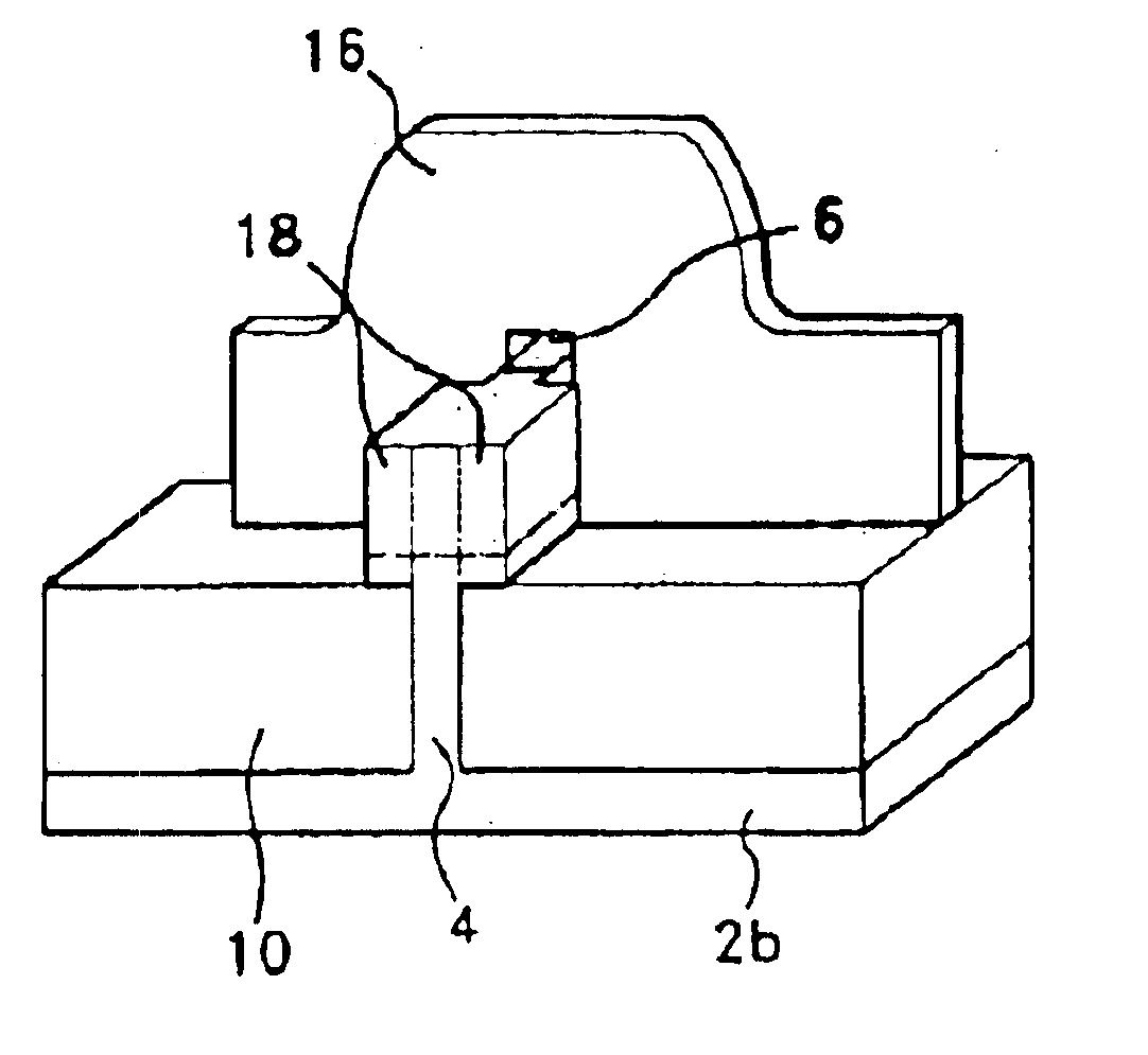
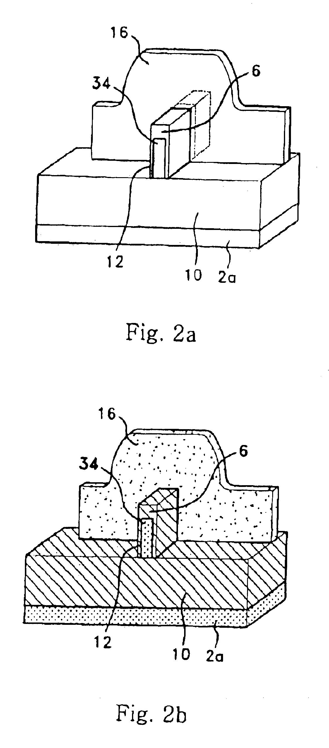
[0062]First of all, the present invention comprises a bulk silicon substrate 2b and a Fin active region 4 which consists of single crystalline silicon with the shape of a wall on the surface of the bulk silicon substrate 2b and is connected to the bulk silicon substrate 2b, a second oxide layer 10 which is formed to a certain height above the Fin active region 4 from the surface of the bulk silicon substrate 2b, a gate oxide layer 12 which is formed at both side-walls of the Fin active region 4 protruded from the second oxide layer 10, a first oxide layer 6 which is formed on the upper surface of the Fin active region 4 with a thickness that is greater or equal to the thickness of the gate oxide 12, a gate 16 which is formed on the first oxide layer 6 and second oxide layer 10, a source / drain region which is formed on both sides of the Fin active ...


PUM


Abstract

The present invention relates to double-gate FinFET devices and fabricating methods thereof. More particularly, the invention relates to an electrically stable double-gate FinFET device and the method of fabrication in which the Fin active region on a bulk silicon substrate where device channel and the body are to be formed has a nano-size width and is connected to the substrate and is formed with the shape of a wall along the channel length direction.
The conventional double-gate MOS devices are fabricated using SOI wafers which are more expensive than bulk silicon wafers. It also has problems including the floating body effects, larger source/drain parasitic resistance, off-current increase, and deterioration in heat transfer to the substrate.

Description

BACKGROUND OF THE INVENTION[0001]The present invention relates to double-gate FinFET devices and fabricating methods thereof. More particularly, the invention relates to an electrically stable double-gate FinFET device and the method of fabrication in which the Fin active region on a bulk silicon substrate where device channel and the body are to be formed has a nano-size width and is connected to the substrate and is formed with the shape of a wall along the channel length direction (the current flow direction).[0002]Worldwide researches are actively being undertaken in the area of nano-CMOS device technologies since the applications of nano-CMOS technologies in logic circuits and memories have the capability of creating substantial value added revenues.[0003]The system based on the silicon semiconductor technology is becoming smaller and requires low electric power consumption. The size of its devices should be small accordingly.[0004]The most competitive device technology which c...

Claims


Application Information

Patent Timeline
IPC IPC(8): H01L29/66H01L29/72H01L27/108H01L21/336H01L29/786
CPCH01L29/41791H01L29/7851H01L29/66795H01L2029/7858
Inventor LEE, JONG-HO
Owner KIPB LLC
Why Eureka
Try Eureka