Method of obtaining a particle-optical image of a sample in a particle-optical device

a particle-optical device and sample technology, applied in the direction of material analysis using wave/particle radiation, instruments, nuclear engineering, etc., can solve the problems of easy to miss electron-optical images, difficult, often impossible, to find the right location in which to make a cross-section, etc., to achieve accurate regulation, easy to knock out places, and easy to regulate

Inactive Publication Date: 2005-05-03
FEI CO
View PDF7 Cites 19 Cited by
  • Summary
  • Abstract
  • Description
  • Claims
  • Application Information

AI Technical Summary

Benefits of technology

[0014]In yet another embodiment of the invention, the ions in the ion beam are heavier than oxygen atoms. As a result of the relatively large mass of the ions, oxygen atoms in the water (or another matrix liquid, such as alcohol) are easily knocked out of places as a result of which a high-speed milling process is achieved.
[0015]In yet another embodiment of the invention, the speed of sublimation is regulated by varying the solid angle at which the cooled opposing surface is seen from the sample. This embodiment is of advantage when, for example, liquid nitrogen is used to cool the opposing surface. The temperature of the opposing surface is then determined by the boiling point of the nitrogen, and is therefore not easy to regulate. By displacing the opposing surface toward or away from the sample, said solid angle is varied, along with the number of captured water molecules and, consequently, the speed of sublimation. In this manner, an accurate regulation of this speed becomes possible.
[0016]In yet another embodiment of the invention, after performing imaging with the aid of a scanning focused electron beam, an ion milling process and a sublimation process are performed anew, after which imaging of at least a portion of the newly exposed cross-section of the sample thus obtained is performed anew with the aid of a scanning focused electron beam. In this manner, it is possible to make a series of SEM images with a steadily (somewhat) advanced erosion front whereby the time between two consecutive images is short as a result of the relatively high speed of the ion milling process, and the distance between two imaging cross-sections can be determined extremely accurately as a result of the high accuracy of the milling process and the sublimation process. In this manner, a three-dimensional re-construction can be made with SEM images.

Problems solved by technology

When using relatively thick samples (i.e. with a thickness of the order of 0.1 mm) in particle-optical devices such as electron microscopes, one can be confronted with the problem that the details to be studied in the sample are located on the interior of the material of the sample.
The device user may suspect that a detail that is of possible interest is situated at a given location on the interior of the sample, but this detail is buried in the bulk of the material and is thus out of the reach of electron-optical imagery using, for example, a Scanning Electron Microscope (SEM).
One could conceive, in a separate operation outside the electron microscope, attempting to open up the sample in such a manner that the detail of interest becomes exposed, but, because the detail involved is often smaller than the wavelength of visible light, the processing thereof is obscured from direct observation by the person performing the processing, so that, in the exposure attempt, the detail of interest can easily be missed, or exposed in an undesirable manner.
Moreover, it is extremely difficult, and often impossible, to find the right location in which to make a cross-section.

Method used


Image

  • Method of obtaining a particle-optical image of a sample in a particle-optical device
  • Method of obtaining a particle-optical image of a sample in a particle-optical device
  • Method of obtaining a particle-optical image of a sample in a particle-optical device

Examples


Embodiment Construction

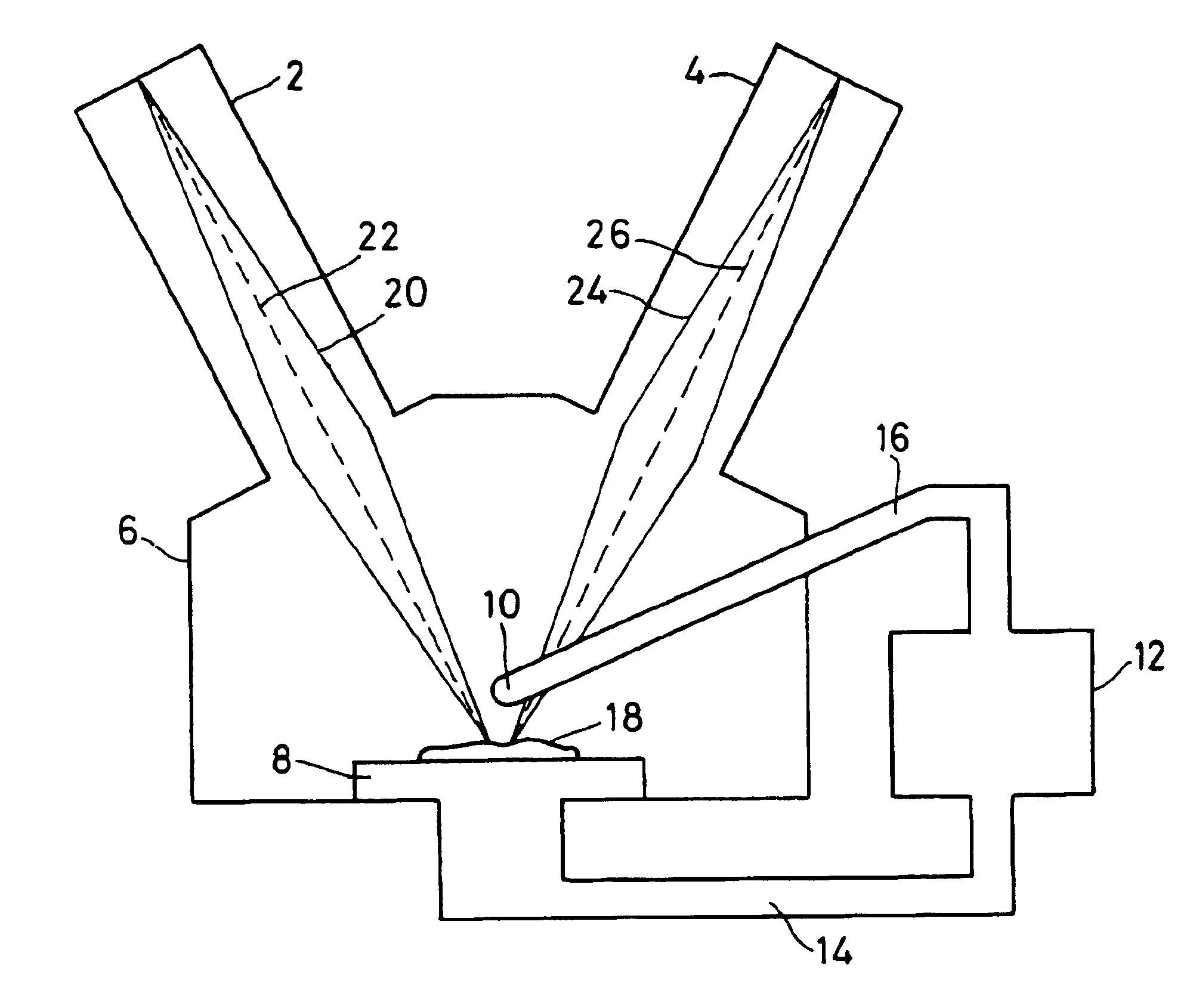
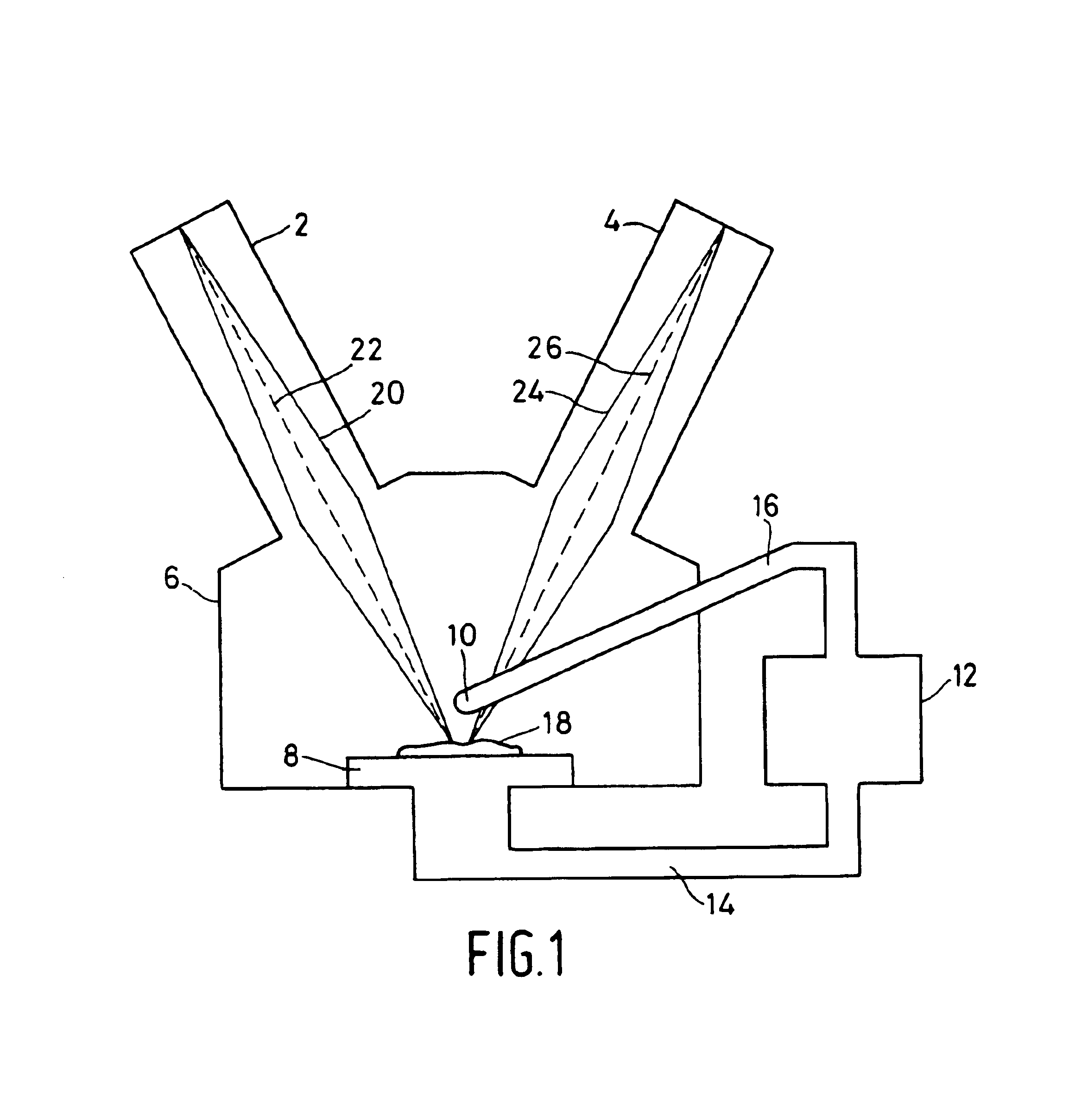
[0022]FIG. 1 schematically depicts a particle-optical device for performing the method according to the invention. The device is formed by a so-called Dual Beam system, in which two particle-optical columns 2 and 4 are present, whereby column 2 is an ion-optical column and column 4 is an electron-optical column. Both columns 2 and 4 are mounted to a sample space 6 that can be evacuated and in which a sample stage 8 is present. The sample space 6 is also provided with a cooled opposing surface in the form of a coo ling finger 10. The sample stage 8 and the cooling finger 10 can be adjusted to a desired low temperature by means of a schematically depicted cooling installation 12. The connection between the cooling installation 12 and the sample stage 8 is schematically depicted by cooling duct 14, and that between the cooling installation 12 and the cooling finger 10 by cooling duct 16. The sample 18 that is to be processed is located on the sample stage.

[0023]Column 2 produces an ion...


PUM

PropertyMeasurementUnit
thicknessaaaaaaaaaa
pressureaaaaaaaaaa
temperatureaaaaaaaaaa

Abstract

In relatively thick samples for electron microscopy imaging, details of interest are often located in the bulk of the sample, so that they cannot be directly imaged in the form of a SEM image. According to the invention, so as to expose the cross-section containing the details of interest, the frozen sample is subjected to ion milling, in such a manner that the desired cross-section is exposed. Thereafter, the exposed cross-section is further eroded in a controlled manner via sublimation, whereby the detail of interest is approached in a very accurate manner, and its fine details become visible. Hereafter, the finally desired SEM image can be made. By repetition of this process, a large number of successive cross-sections can be imaged, so that a spatial representation of the sample is obtained.

Description

FIELD OF THE INVENTION[0001]The invention relates to method of obtaining a particle-optical image of a sample in a particle-optical device. The invention also relates to a particle-optical device embodied to perform the method.BACKGROUND OF THE INVENTION[0002]When using relatively thick samples (i.e. with a thickness of the order of 0.1 mm) in particle-optical devices such as electron microscopes, one can be confronted with the problem that the details to be studied in the sample are located on the interior of the material of the sample. Such a situation can, for example, arise when using a bacterium as a sample, whereby one would like to subject a detail to further analysis using a (much) stronger magnification in the electron microscope. The device user may suspect that a detail that is of possible interest is situated at a given location on the interior of the sample, but this detail is buried in the bulk of the material and is thus out of the reach of electron-optical imagery us...

Claims


Application Information

Patent Timeline
Patent Type & Authority Patents(United States)
IPC IPC(8): G01N1/42G01N1/32H01J37/28G01N23/225G01N1/28H01J37/317
CPCG01N1/32H01J37/28G01N1/42H01J2237/2001
Inventor GEURTS, REMCO THEODORUS JOHANNES PETRUSHAYLES, MICHAEL FREDERICK
Owner FEI CO
Why Eureka
Try Eureka