Integrated sensor and electronics package

a sensor and electronics technology, applied in the direction of fluid pressure measurement, printed circuit non-printed electric components association, instruments, etc., can solve the problems of achieve the effect of reducing parasitic capacitance and noise susceptibility, and reducing the path length of electrical interconnections

Inactive Publication Date: 2005-05-10
CHARLES STARK DRAPER LABORATORY
View PDF4 Cites 68 Cited by
  • Summary
  • Abstract
  • Description
  • Claims
  • Application Information

AI Technical Summary

Benefits of technology

[0007]It is therefore an object of this invention to further reduce the path length of the electrical interconnections associated with sensors and their controlling electronics to thereby reduce parasitic capacitance and noise susceptibility.
[0008]It is a further object of this invention to reduce the number of electrical interconnections associated with various kinds of sensors and their controlling electronics.
[0009]It is a further object of this invention to provide a compact integrated sensor and electronics package.
[0010]It is a further object of this invention to provide a complete accelerometer or gyroscope system with better performance.
[0011]This invention results from the realization that an integrated sensor and electronics package is effected by mounting the sensor die directly on one side of the substrate of a package and stacking the ASIC and digital gate array chips on the opposite side of the substrate package to eliminate entirely the prior art ceramic leadless sensor chip carrier and the electrical interconnections between the sensor die and the ceramic leadless sensor chip carrier and also to greatly reduce the length of the electrical interconnections between the ASIC chip and the digital gate array chip and also between the sensor chip and the ASIC chip.

Problems solved by technology

As the sensors are made more sensitive, however, parasitic capacitance and noise are still problems.

Method used


Image

  • Integrated sensor and electronics package
  • Integrated sensor and electronics package
  • Integrated sensor and electronics package

Examples


Embodiment Construction

[0035]Aside from the preferred embodiment or embodiments disclosed below, this invention is capable of other embodiments and of being practiced or being carried out in various ways. Thus, it is to be understood that the invention is not limited in its application to the details of construction and the arrangements of components set forth in the following description or illustrated in the drawings.

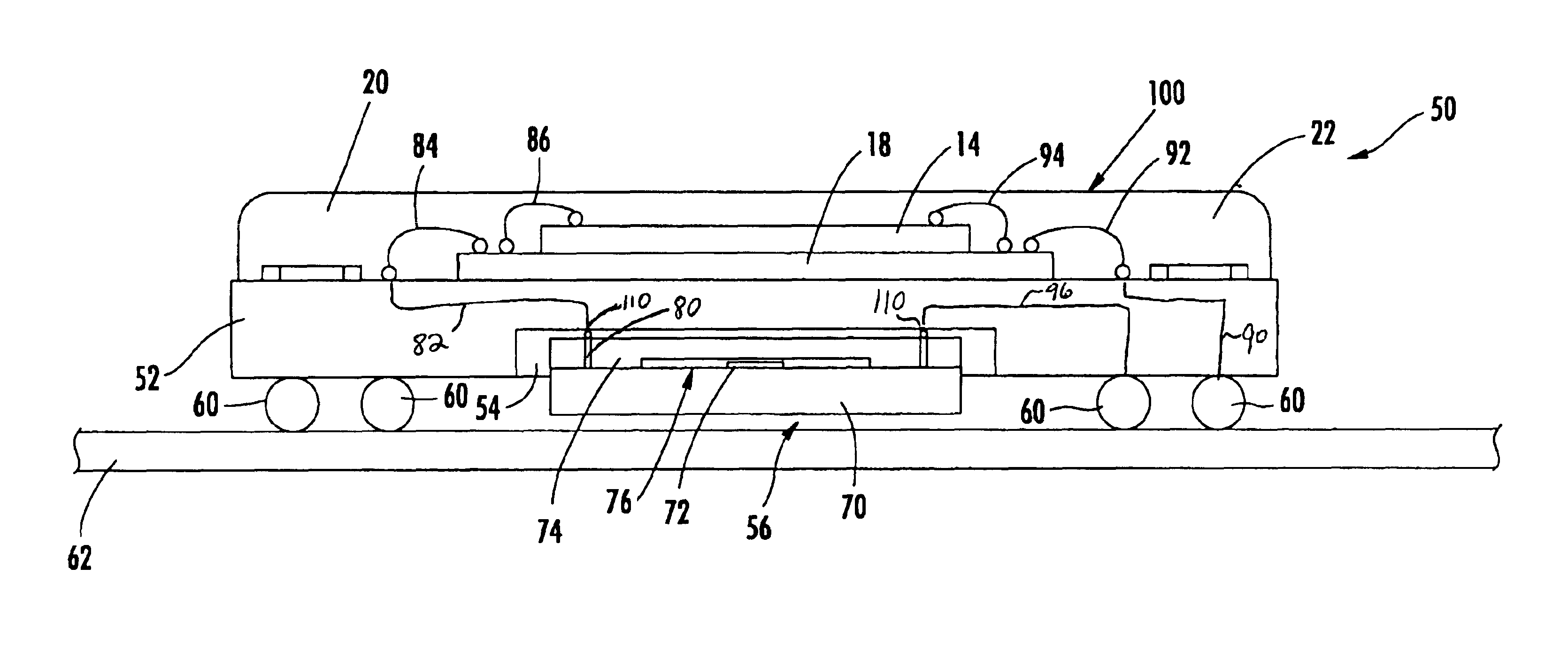
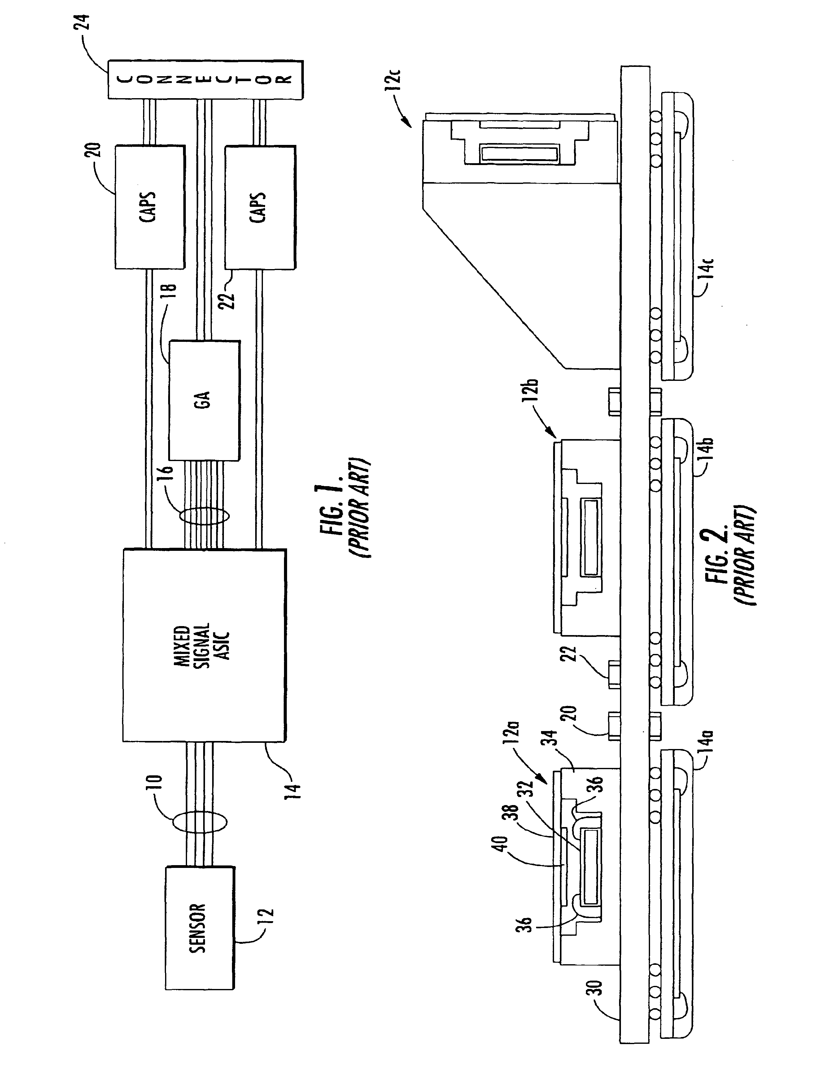
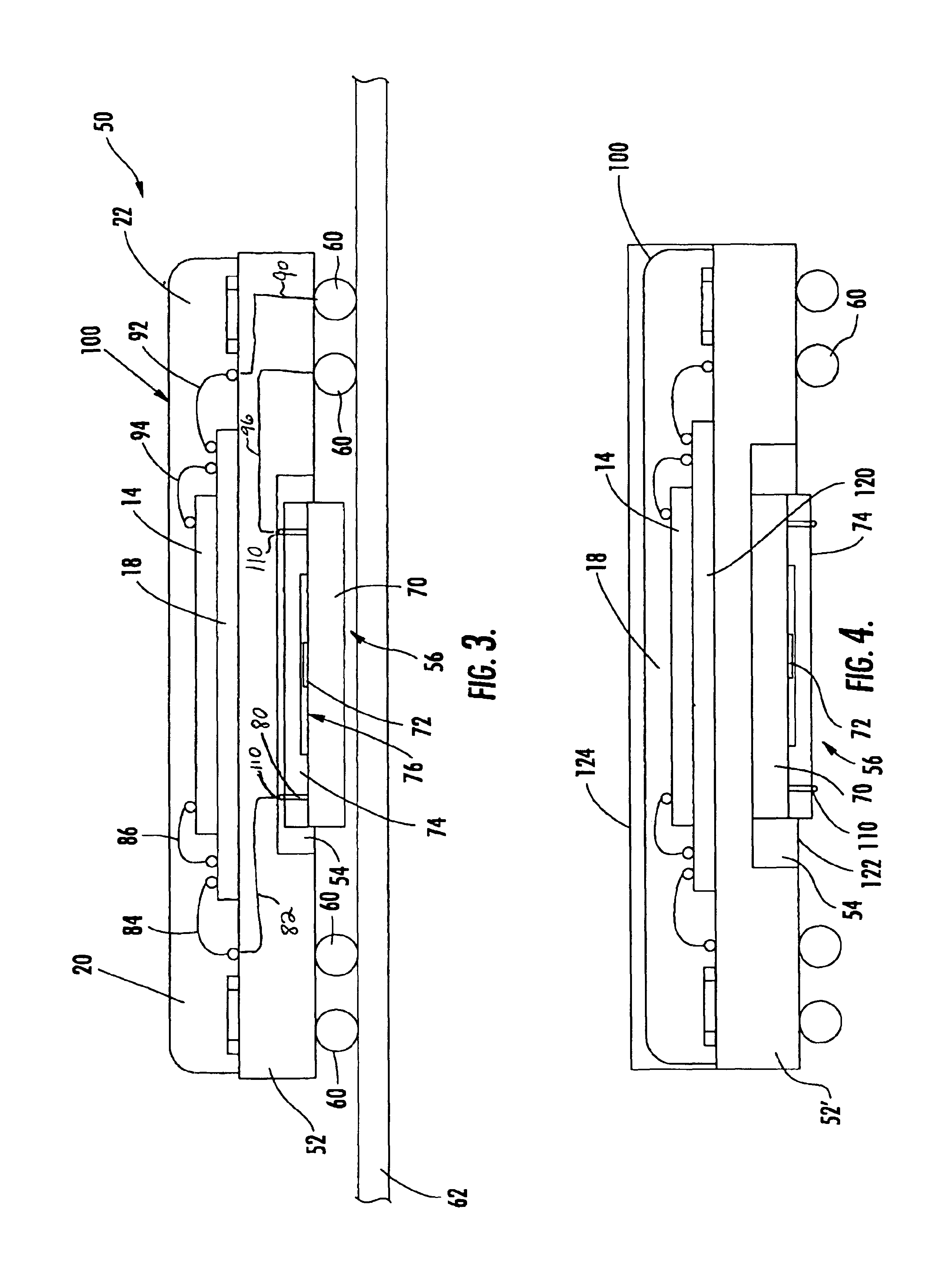
[0036]As discussed in the Background section above, there may be eight to twelve electrical interconnections 10, FIG. 1 between sensor 12 and mixed signal ASIC chip 14 and many (one hundred or more) electrical interconnections 16 between ASIC 14, and digital gate array chip 18. Also shown in FIG. 1 are decoupling capacitor chips 20 and 22, the electrical connections between decoupling capacitor chips 20 and 22 and ASIC 14, and connector 24 electrically connected to decoupling capacitors 20, 22, and digital gate array chip 18.

[0037]Those skilled in the art have attempted to minimize the leng...


PUM

PropertyMeasurementUnit
diameteraaaaaaaaaa
temperatureaaaaaaaaaa
lengthaaaaaaaaaa

Abstract

An integrated sensor and electronics package wherein a micro-electromechanical sensor die is bonded to one side of the package substrate, one or more electronic chips are bonded to an opposite side of the package substrate, internal electrical connections run from the sensor die, through the package substrate, and to the one or more electronic chips, and input / output connections on the package substrate are electrically connected to one or more of the electronic chips.

Description

RELATED APPLICATIONS[0001]This application claims priority of U.S. Provisional Application No. 60 / 362,367 filed Mar. 6, 2002.FIELD OF THE INVENTION[0002]This invention relates to an integrated sensor and electronics package.BACKGROUND OF THE INVENTION[0003]A complete accelerometer typically includes three micro-electromechanical (MEM) dies each mounted in a ceramic leadless chip carrier package forming a sensor chip mounted on a printed circuit board. Application specific integrated circuit (ASIC) chips, one for controlling each sensor die, are also mounted on the printed circuit board as are digital gate array chips and decoupling capacitor chips. Typically, there are numerous electrical interconnections between each sensor chip and each ASIC chip and many (a hundred or more) electrical interconnections between each ASIC chip and each digital gate array chip.[0004]Those skilled in the art understand that the sensor chip packages must be mounted in close proximity to the respective ...

Claims


Application Information

Patent Timeline
Patent Type & Authority Patents(United States)
IPC IPC(8): H01L27/14B81B7/00H05K
CPCB81B7/007H01L2224/48091H01L2924/00014
Inventor ANDERSON, RICHARD S.CONNELLY, JAMES H.HANSON, DAVID S.SOUCY, JOSEPH W.MARINIS, THOMAS F.
Owner CHARLES STARK DRAPER LABORATORY
Why Eureka
Try Eureka