Fabrication process of a semiconductor device including a CVD process of a metal film

a technology of metal film and fabrication process, which is applied in the direction of semiconductor/solid-state device details, chemical vapor deposition coating, coating, etc., can solve the problems of metal film peeling off, disconnection or short-circuit, poor adhesion between metal film and cvd process

Inactive Publication Date: 2005-05-17
TOKYO ELECTRON LTD
View PDF8 Cites 16 Cited by
  • Summary
  • Abstract
  • Description
  • Claims
  • Application Information

AI Technical Summary

Benefits of technology

[0011]Accordingly, it is a general object of the present invention to provide a novel and usef

Problems solved by technology

On the other hand, the use of such a metal film formed by a CVD process raises the problem of peeling-off of the metal film, particularly when a CMP process is applied thereto in a process such as a dual damascene process.
Further, such a poor adhesion between the metal film and the barrier conductor layer can become the cause of disconnection or short-

Method used


Image

  • Fabrication process of a semiconductor device including a CVD process of a metal film
  • Fabrication process of a semiconductor device including a CVD process of a metal film
  • Fabrication process of a semiconductor device including a CVD process of a metal film

Examples


first embodiment

[First Embodiment]

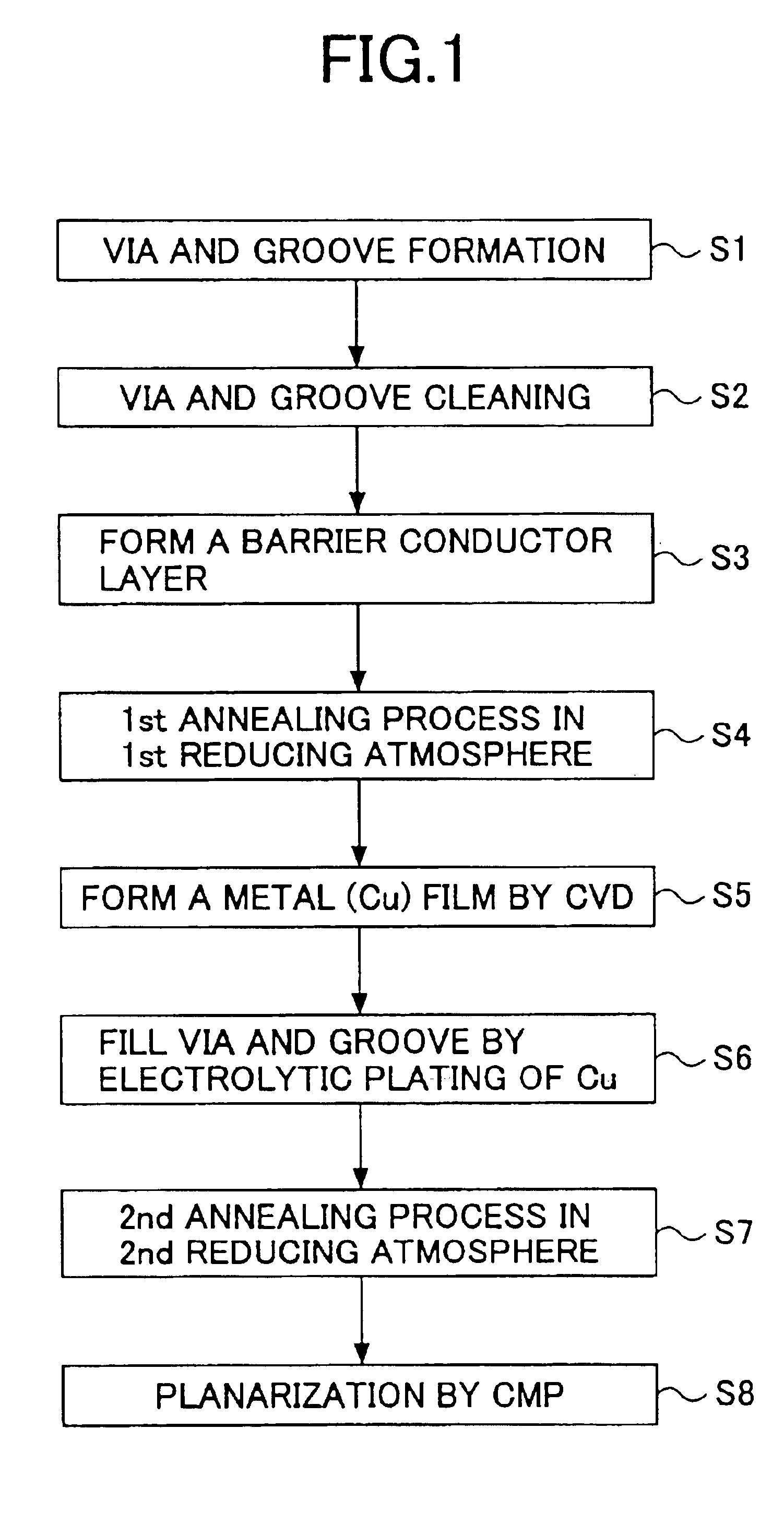
[0035]Hereinafter, the fabrication process of a semiconductor device according to a first embodiment of the present invention will be described with reference to FIG. 1 showing a flowchart and FIGS. 2-9 showing a process flow of the fabrication process of the semiconductor device.

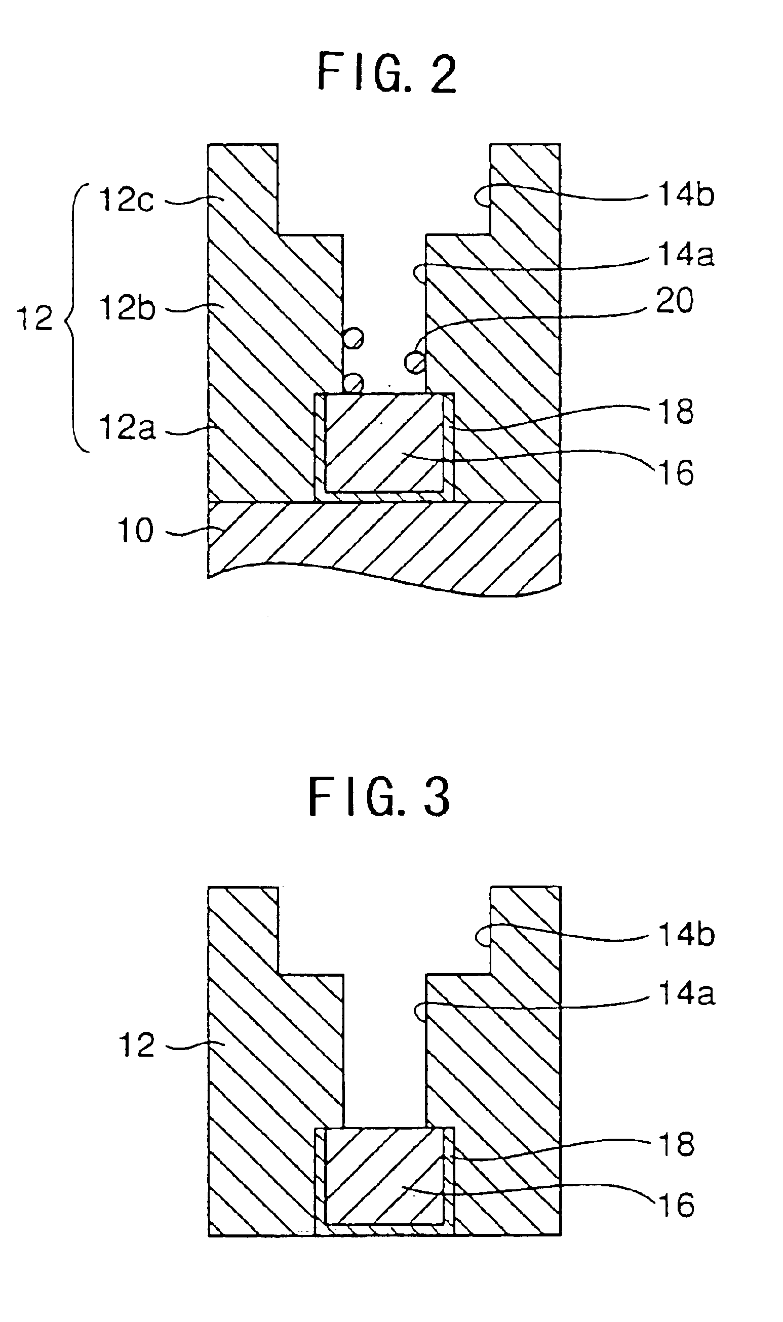
[0036]Referring to the flowchart of FIG. 1, the process starts with a step S1 in which a Si substrate 10 is covered by a plurality of insulating films 12a-12c consecutively as represented in FIG. 2, with intervening etching stopper films not illustrated. For the sake of simplicity, the insulating films 12a-12c are collectively designated by a reference numeral 12. In the step S1 corresponding to FIG. 2, a via hole 14a for a conductor plug and a groove 14b for an interconnection pattern are formed by an etching process. Thereby, the via hole 14a and the groove 14b form together a stepped structure in the cross-section of FIG. 2.

[0037]In the structure of FIG. 2, it should be noted that there...

second embodiment

[Second Embodiment]

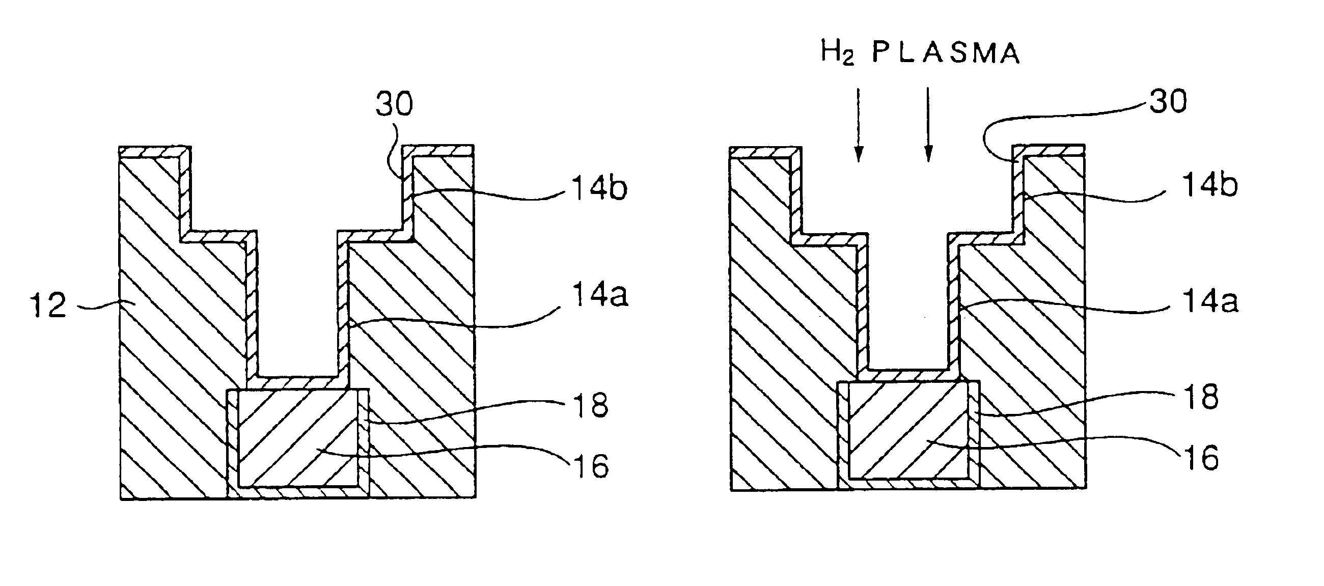
[0047]Next, the semiconductor fabrication process according to a second embodiment of the present invention will be described with reference to FIG. 10 showing a flowchart and FIGS. 11-18 showing the process flow. In the drawings, those parts corresponding to the parts described previously are designated by the same reference numerals and the description thereof will be omitted.

[0048]Referring to FIG. 11 corresponding to the step S11 of FIG. 10, the via hole 14a for a conductor plug and the groove pattern 14b corresponding to an interconnection pattern are formed in the insulating film 12.

[0049]Next, in the step of FIG. 12 corresponding to the step S12 of FIG. 10, the via hole 14a and the groove 14b are subjected to a cleaning process.

[0050]Next, a barrier conductor layer 30 of WN is formed in the step of FIG. 13 corresponding to the step S13 of FIG. 10 such that the barrier conductor layer 30 covers the sidewalls of the via hole 14a and the groove 14b and further...


PUM

PropertyMeasurementUnit
Temperatureaaaaaaaaaa
Pressureaaaaaaaaaa

Abstract

A method for fabricating a semiconductor device includes the steps of forming a barrier conductor layer on a substrate, exposing the barrier conductor layer to a first reducing gas atmosphere at an elevated substrate temperature, forming a metal film on the barrier conductor layer by a CVD process, and exposing the metal film to a second gas atmosphere at an elevated substrate temperature.

Description

CROSS-REFERENCE TO RELATED APPLICATIONS[0001]The present invention is based on Japanese Priority Application 2000-115187 filed on Apr. 17, 2000, the entire contents thereof are incorporated herein by reference.BACKGROUND OF THE INVENTION[0002]The present invention generally relates to fabrication of semiconductor devices and more particularly to a fabrication process of a semiconductor device including the step of forming a metal film on a barrier conductor layer by way of a CVD process.[0003]In the fabrication process of semiconductor devices such as a wafer process, various metal films or patterns are formed on a substrate such as a Si wafer or a glass slab for providing interconnection. In the process of forming such metal films, it is practiced to provide a barrier conductor layer between the metal film and the underlying insulating layer such that diffusion of metal ions from the metal film into the underlying insulating layer is effectively blocked. Although the barrier conduc...

Claims


Application Information

Patent Timeline
IPC IPC(8): H01L21/285H01L21/02H01L21/70H01L21/768H01L21/311C25D7/12C23C16/02C23C16/56H01L21/28H01L21/3205H01L23/52
CPCH01L21/2855H01L21/28556H01L21/76877H01L21/76862H01L21/76864H01L21/76873H01L21/76843H01L21/31116
Inventor HOSHINO, TOMOHISAVEZIN, VINCENTCHUNG, GISHI
Owner TOKYO ELECTRON LTD
Why Eureka
Try Eureka