Gate stack for high performance sub-micron CMOS devices

a technology of cmos and gate stacks, applied in the direction of semiconductor devices, electrical apparatus, transistors, etc., can solve the problems of excessive dc power consumption, scaling of the thickness of the gate oxide layer, scaling of the width of the spacer, etc., to increase the drive current capability, reduce the impact of parasitic capacitance, and increase the inversion carrier density

Inactive Publication Date: 2005-05-17
TAIWAN SEMICON MFG CO LTD
View PDF20 Cites 39 Cited by
  • Summary
  • Abstract
  • Description
  • Claims
  • Application Information

AI Technical Summary

Benefits of technology

[0016]A still further objective of the invention is to provide a gate electrode structure having sub-micron device feature lengths of increased drive current capability.
[0017]A still further objective of the invention is to provide a gate electrode structure having sub-micron device feature lengths of reduced parasitic capacitance impact.
[0018]In accordance with the objectives of the invention a new method is provided for the creation of sub-micron gate electrode structures. A high-k dielectric is used for the gate dielectric, providing increased inversion carrier density without having to resort to aggressive

Problems solved by technology

For this reason a thin layer of silicon dioxide (thinner than about 1.5 nm) may lead to excessive DC power consumption and is not widely used in power sensitive circuits or products.
The conventional approach of using a layer of silicon oxide, over which the gate electrode is created, and of using silicon nitride for the gate s

Method used


Image

  • Gate stack for high performance sub-micron CMOS devices
  • Gate stack for high performance sub-micron CMOS devices
  • Gate stack for high performance sub-micron CMOS devices

Examples


Embodiment Construction

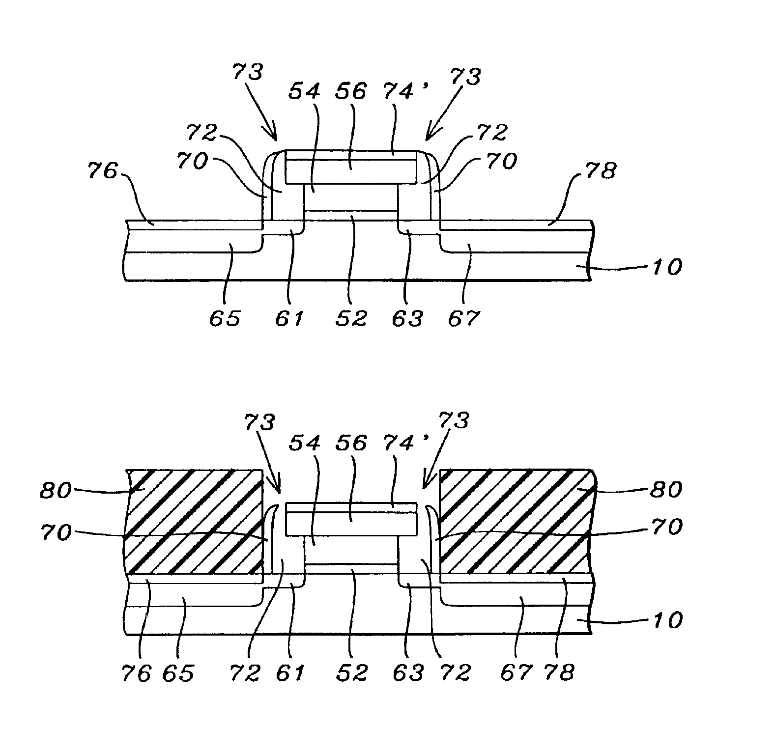
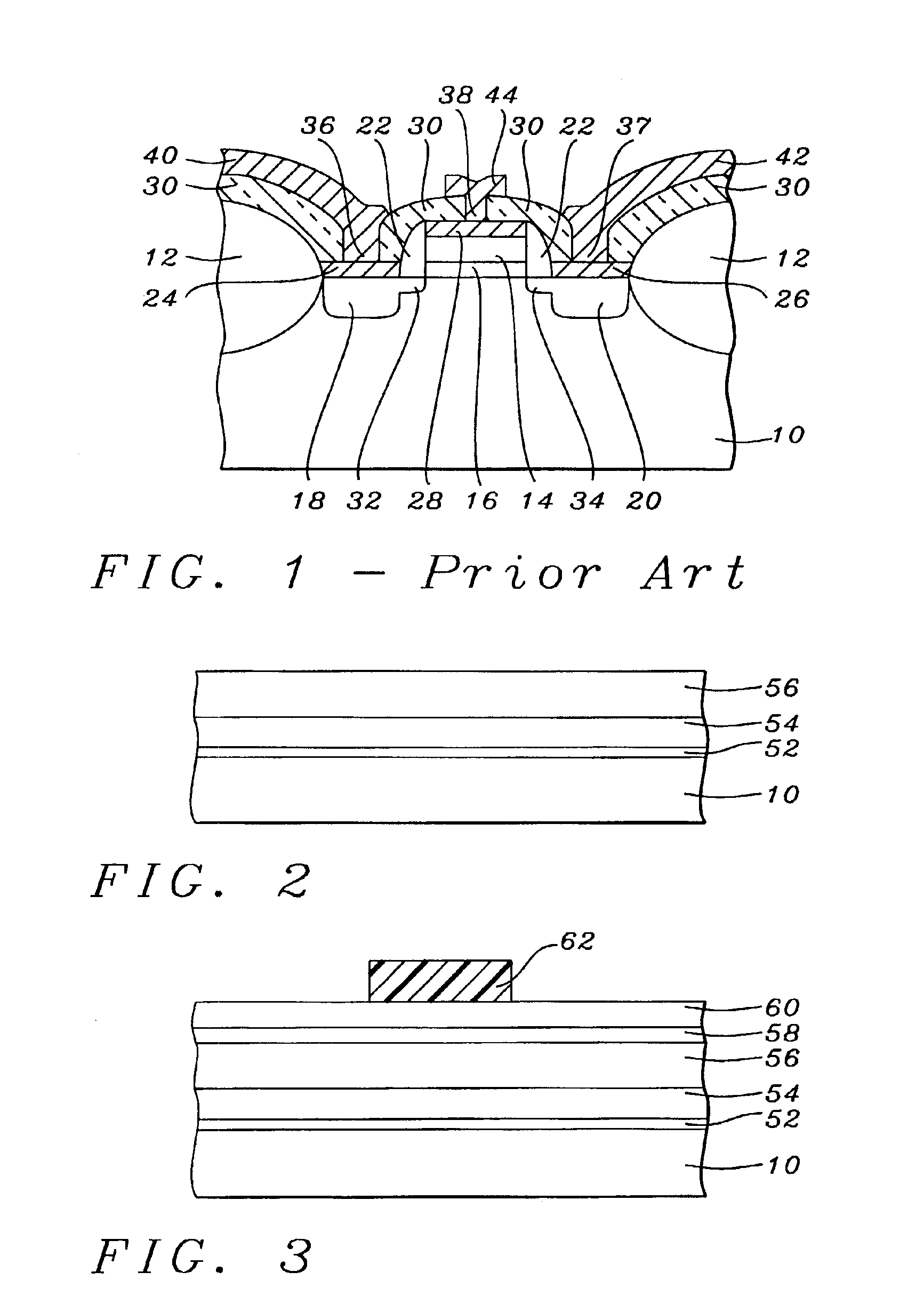
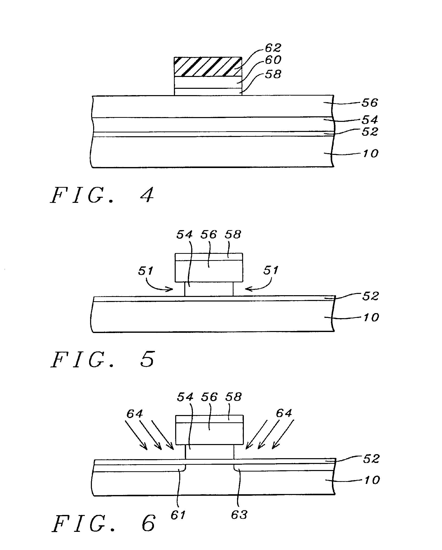
[0034]Some of the essential points that must be addressed in the creation of CMOS devices having sub-micron channel length can be highlighted as follows:[0035]the thickness of the layer of gate oxide must be made as small as possible since the drive current of a CMOS device increases with decreasing thickness of the layer of gate oxide; a thin layer of gate oxide allows the gate to retain strong control of the channel charge region underneath the gate electrode[0036]shallow junction depths are required for the device impurity implants, the shallow junction depth prevents the drain field from extending for into the channel region underneath the gate electrode[0037]the thin layer of gate dielectric must be grown over the surface of the substrate in a uniform manner, this to prevent uneven distribution of the electromagnetic field between the gate electrode and the channel region of the gate electrode[0038]the impurity content of the layer of gate dielectric must be very low to prevent...


PUM


Abstract

A new method is provided for the creation of sub-micron gate electrode structures. A high-k dielectric is used for the gate dielectric, providing increased inversion carrier density without having to resort to aggressive scaling of the thickness of the gate dielectric while at the same time preventing excessive gate leakage current from occurring. Further, air-gap spacers are formed over a stacked gate structure. The gate structure consists of pre-doped polysilicon of polysilicon-germanium, thus maintaining superior control over channel inversion carriers. The vertical field between the gate structure and the channel region of the gate is maximized by the high-k gate dielectric, capacitive coupling between the source/drain regions of the structure and the gate electrode is minimized by the gate spacers that contain an air gap.

Description

[0001]This is a division of patent application Ser. No. 09 / 905,403, filing date Jul. 16, 2001 U.S. Pat. No. 6,596,599, New Gate Stack For High Performance Sub-Micron Cmos Devices, assigned to the same assignee as the present invention.BACKGROUND OF THE INVENTION[0002](1) Field of the Invention[0003]The invention relates to the fabrication of integrated circuit devices, and more particularly, to a method of creating a gate electrode for CMOS devices having sub-micron channel length.[0004](2) Description of the Prior Art[0005]CMOS devices, which form the essential components of logic circuits and Si memory cells, are typically created using overlying layers of semiconductor material with the lowest layer being a layer of pad oxide and the highest layer being a layer of silicided material that serves as low resistivity electrical contact to the gate electrode. A gate electrode is typically created overlying the layer of pad oxide, this layer is also referred to as gate dielectric or ga...

Claims


Application Information

Patent Timeline
IPC IPC(8): H01L21/02H01L21/336H01L21/4763H01L21/70H01L21/3205H01L21/8238H01L21/265H01L21/28H01L29/49
CPCH01L21/28114H01L29/6659H01L29/4991H01L29/4983H01L21/26586H01L21/823864H01L29/665
Inventor GUO, JYH-CHYURN
Owner TAIWAN SEMICON MFG CO LTD
Why Eureka
Try Eureka