
Memory array employing single three-terminal non-volatile storage elements

a technology of non-volatile storage elements and memory arrays, which is applied in the field of memory circuits, can solve the problems of coupled noise generation, coupled noise sensitivity, and dram-like cell structure, and achieve the effect of improving non-volatile memory arrays and denser memory arrays

Inactive Publication Date: 2005-05-17
IBM CORP
View PDF17 Cites 59 Cited by
  • Summary
  • Abstract
  • Description
  • Claims
  • Application Information

AI Technical Summary

Benefits of technology

[0007]The present invention provides an improved non-volatile memory array which eliminates at least some of the disadvantages present in conventional non-volatile memory arrays. The memory array of the invention utilizes ferroelectric memory cells which include a single ferroelectric device, thereby providing a smaller memory cell which, when incorporated into the memory array, advantageously results in a denser memory array compared to conventional memory architectures.
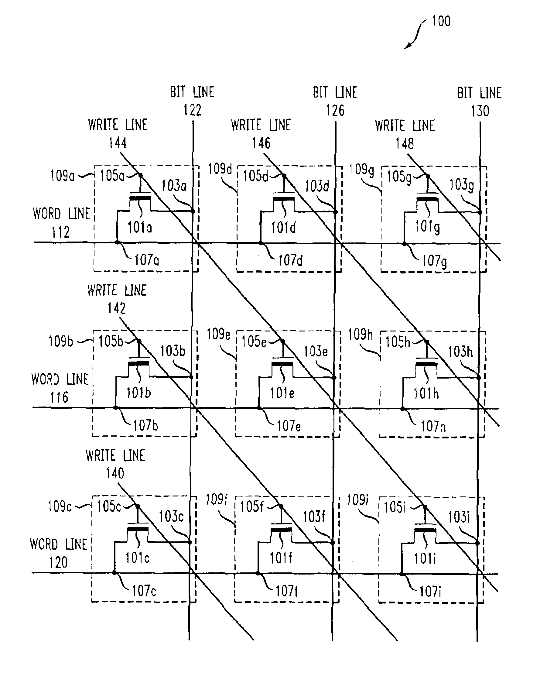
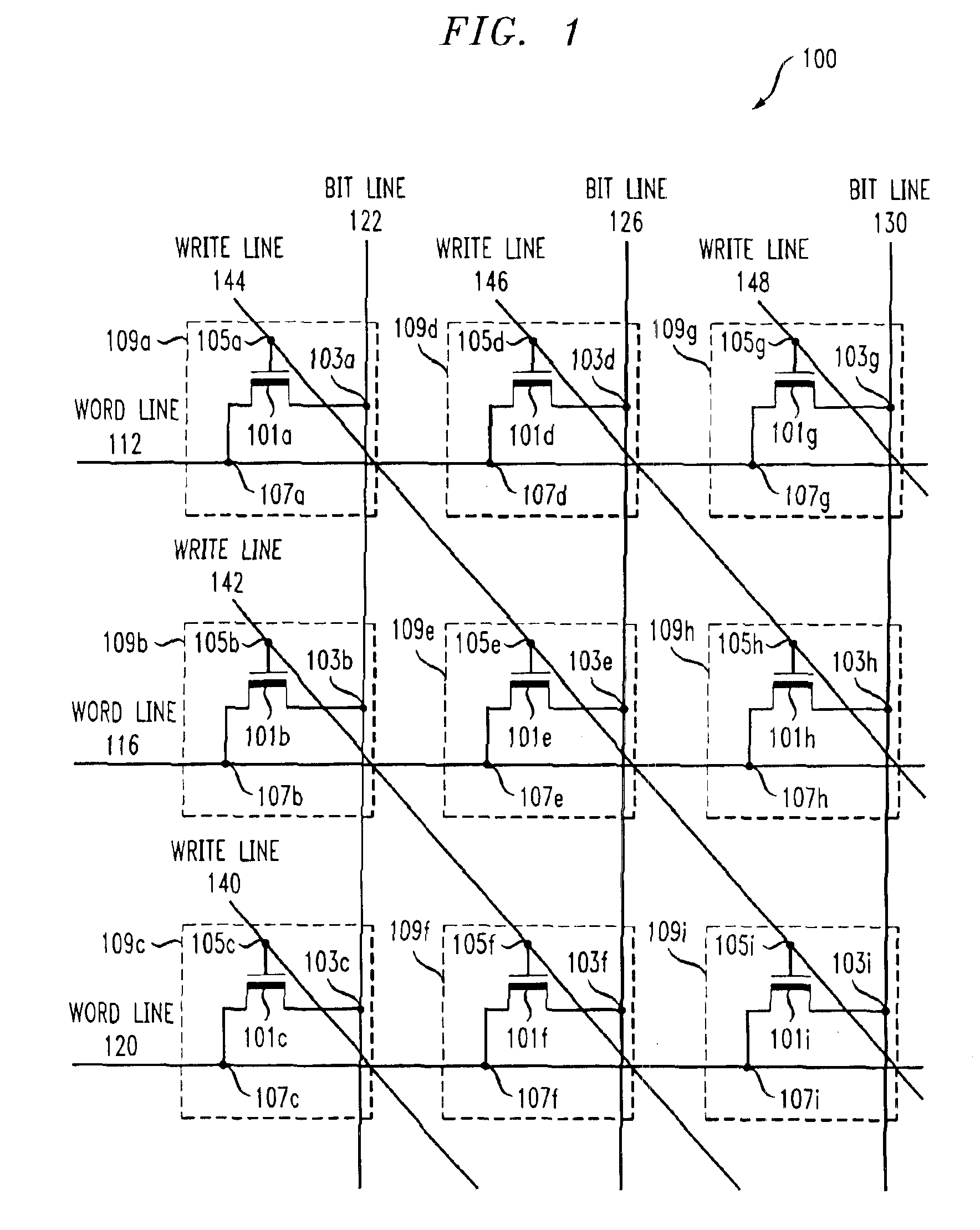
[0008]In accordance with one aspect of the invention, an improved non-volatile memory array comprises a plurality of memory cells, at least one of the memory cells comprising a three-terminal non-volatile storage element for storing a logical state of the at least one memory cell. The memory array further comprises a plurality of write lines operatively coupled to the memory cells for selectively writing the logical state of one or more memory cells in the memory array, and a plurality of bit lines and word lines operatively coupled to the memory cells for selectively reading and writing the logical state of one or more memory cells in the memory array. The memory array is advantageously configured so as to eliminate the need for a pass gate operatively coupled to a corresponding non-volatile storage element in the at least one memory cell.
[0009]In accordance with another aspect of the invention, a method of forming a non-volatile memory array comprises the steps of: providing a plurality of memory cells, at least one memory cell comprising a three-terminal non-volatile storage element for storing a logical state of the at least one memory cell; and coupling the memory cells to a plurality of write lines, bit lines and word lines for selectively reading and writing the logical state of one or more memory cells in the memory array, the memory cells being operatively coupled to the write lines, bit lines and word lines so as to eliminate a need for a pass gate being coupled to a corresponding non-volatile storage element in the at least one memory cell.

Problems solved by technology

Although this type of memory may be easy to fabricate, the DRAM-like cell structure has several disadvantages, including coupled noise sensitivity, coupled noise generation, large power consumption and low overall performance.
The density of the memory device suffers compared to conventional DRAM due, at least in part, to the use of a ferroelectric capacitor plate electrode and the need for a special driver circuit.
Moreover, because the driver circuit must be capable of driving a heavily loaded wire during read and write operations, it is particularly slow.
This results in significant noise coupling between signal lines as well as high power consumption.
Although there has been some recent progress in terms of density, power consumption and material-related problems, several fundamental issues remain in ferroelectric memories exploiting a DRAM-type cell structure which prevent this type of conventional memory from being used in high density, high speed and / or low power applications.

Method used


Image

  • Memory array employing single three-terminal non-volatile storage elements
  • Memory array employing single three-terminal non-volatile storage elements
  • Memory array employing single three-terminal non-volatile storage elements

Examples


Embodiment Construction

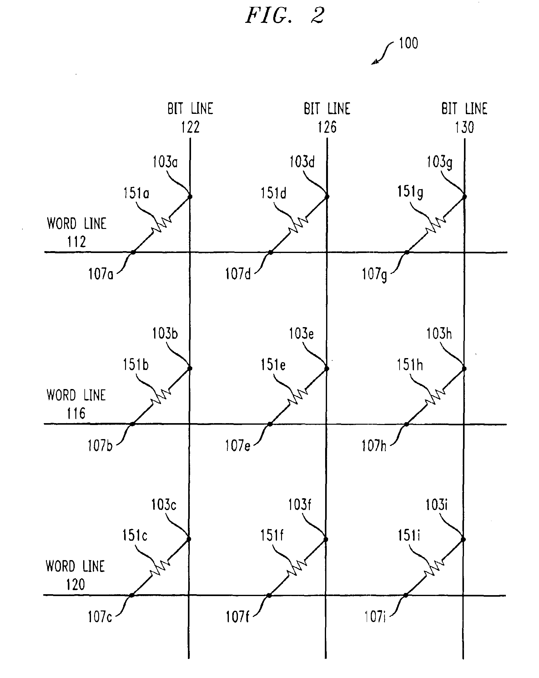
[0019]The present invention will be described herein in the context of a memory architecture employing a plurality of memory cells, each of the memory cells comprising a single ferroelectric gate field-effect transistor (FeGFET) device. The FeGFET device in each memory cell serves as a non-volatile storage element, retaining the logical state of a given cell without an expenditure of energy. It should be appreciated, however, that the present invention is not limited to this or any particular memory architecture. Rather, the invention is more generally applicable to providing a non-volatile memory architecture that is configured so as to advantageously eliminate the need for a pass gate being coupled to the storage element in at least a portion of the memory cells. Moreover, the present invention is not limited to FeGFET devices used as a memory cell. Instead, any three-terminal storage element exhibiting a variable resistance change caused by an applied electric field may be employ...


PUM


Abstract

An improved non-volatile memory array comprises a plurality of memory cells, at least one of the memory cells comprising a three-terminal non-volatile storage element for storing a logical state of the at least one memory cell. The memory array further comprises a plurality of write lines operatively coupled to the memory cells for selectively writing the logical state of one or more memory cells in the memory array, and a plurality of bit lines and word lines operatively coupled to the memory cells for selectively reading and writing the logical state of one or more memory cells in the memory array. The memory array is advantageously configured so as to eliminate the need for a pass gate being operatively coupled to a corresponding non-volatile storage element in the at least one memory cell.

Description

CROSS-REFERENCE TO RELATED APPLICATIONS[0001]The present application is related to the U.S. patent application identified by Ser. No. 10 / 256,881 and entitled “Non-Volatile Memory Using Ferroelectric Gate Field-Effect Transistors,” which is filed concurrently herewith and incorporated herein by reference.FIELD OF THE INVENTION[0002]The present invention relates generally to memory circuits, and more particularly relates to a memory array comprising a plurality of three-terminal non-volatile storage elements.BACKGROUND OF THE INVENTION[0003]Using ferroelectric material in the manufacture of non-volatile memories has been well-established. For instance, U.S. Pat. No. 3,832,700 issued to Wu et al. describes a ferroelectric memory device which utilizes remnant polarization of a ferroelectric film as the storage mechanism. This structure may be considered analogous to a conventional electrically erasable programmable read-only memory (EEPROM). U.S. Pat. No. 4,873,664 issued to Eaton, Jr. ...

Claims


Application Information

Patent Timeline
IPC IPC(8): G11C11/22H01L21/8246H01L21/8247H01L27/105H01L29/788H01L29/792
CPCG11C11/22
Inventor REOHR, WILLIAM ROBERTWANG, LI-KONG
Owner IBM CORP
Learn More