Supercharge Your Innovation With Domain-Expert AI Agents!

Method of manufacturing a semiconductor device having plural semiconductor chips, wherein electrodes of the semiconductor chips are electrically connected together via wiring substrates of the semiconductor chips

a semiconductor chip and semiconductor technology, applied in semiconductor devices, semiconductor/solid-state device details, electrical equipment, etc., can solve the problems of sacrificing the speed of logic units, increasing the load of semiconductor manufacturing processes, and reducing the efficiency of logic units, so as to improve the packing density, speed up the data transfer rate, and save space

Inactive Publication Date: 2005-05-31
TESSERA ADVANCED TECH
View PDF17 Cites 22 Cited by
  • Summary
  • Abstract
  • Description
  • Claims
  • Application Information

AI Technical Summary

Benefits of technology

[0004]A move attempt to form a microcomputer, a flash memory, a DRAM, an ASIC, etc. on one chip thereby to achieve the speeding up of a data transfer rate, space saving (improvements in packing density), low power consumption, etc. has rece...

Problems solved by technology

However, the formation of such many kinds of LSIs on one chip will cause an extreme increase in the load on a semiconductor manufacturing process.
(1) The attainment of the speeding up of a logic unit needs to shorten a gate length of each MOSFET and thin the thickness of a gate oxide film. On the other hand, it is necessary to make the thickness of a gate oxide film of each MOSFET for a DRAM thicker than that of a gate oxide film of each MOSFET for the logic unit to some extent in consideration of a withstand voltage or high voltage. Further, a gate oxide film of each high-withstand MOSFET for a flash memory to which a high voltage is applied, needs to have a thicker thickness in order to ensure a sufficient withstand voltage. That is, when the DRAM, logic and flash memory are placed in mixed form, it is necessary to provide gate oxide films having thicknesses which vary according to required power levels. Therefore, the number of process steps and the number of masks increase by a large amount.
(2) When a DRAM is comprised of one transistor+one capacitor, a high-temperature heat treatment (corresponding to heat treatment for stabilizing the tantalum oxide film or high-temperature nitriding treatment) is taken upon formation of the capacitor. It is therefore necessary to set the gate length at the logic unit longer more or less However, when the gate length at the logic unit is made longer, the speeding up of the logic unit will fall a sacrifice.
(3) Since the height of the DRAM on the semiconductor chip is higher than the logic unit and there is a step-like offset between the two, this exerts a bad influence on wiring formation. This tendency becomes pronounced in the case of a DRAM which adopts a stacked capacitor (Stacked Capacitor) structure in particular.
Even in either case, the manufacturing cost greatly increases.
According to this method, since the logic circuit of the DRAM on-chip logic outputs a request signal for making a request to the CPU for a bus release and the CPU cannot do anything during a period in which a bus is set free to the logic circuit, the present method will cause a malfunction or inconvenience that overheads of the arbitration increase and the CPU itself cannot perform time-based control.

Method used


Image

  • Method of manufacturing a semiconductor device having plural semiconductor chips, wherein electrodes of the semiconductor chips are electrically connected together via wiring substrates of the semiconductor chips
  • Method of manufacturing a semiconductor device having plural semiconductor chips, wherein electrodes of the semiconductor chips are electrically connected together via wiring substrates of the semiconductor chips
  • Method of manufacturing a semiconductor device having plural semiconductor chips, wherein electrodes of the semiconductor chips are electrically connected together via wiring substrates of the semiconductor chips

Examples


Embodiment Construction

[0063]Preferred embodiments of the present invention will hereinafter be described in detail with reference to the accompanying drawings. Parts or components having the same functions in all the drawings for describing the embodiments are identified by the same reference numerals and their repetitive description will be omitted.

[0064]An example of a configuration of a semiconductor device according to the present embodiment will first be explained with reference to FIGS. 1 through 6.

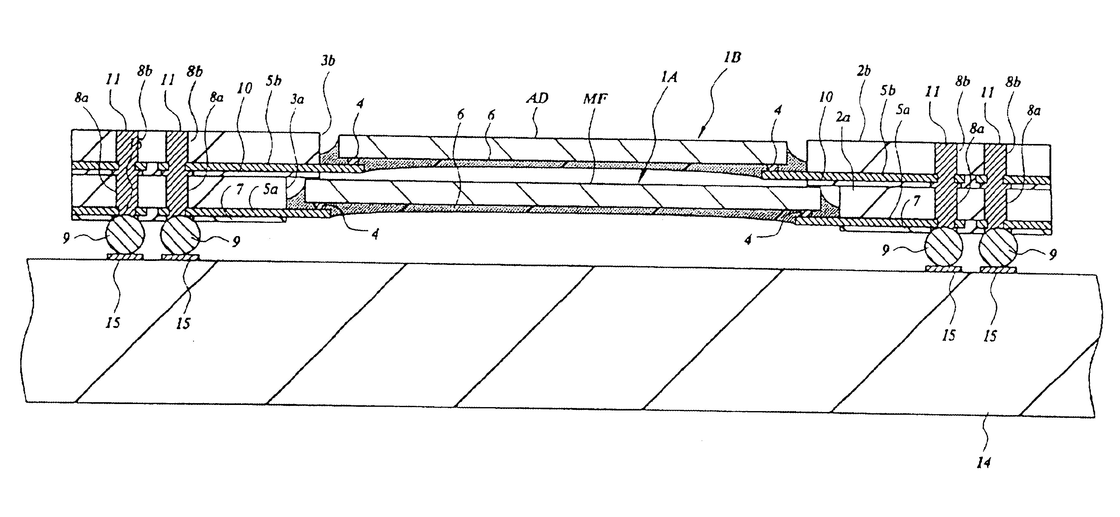
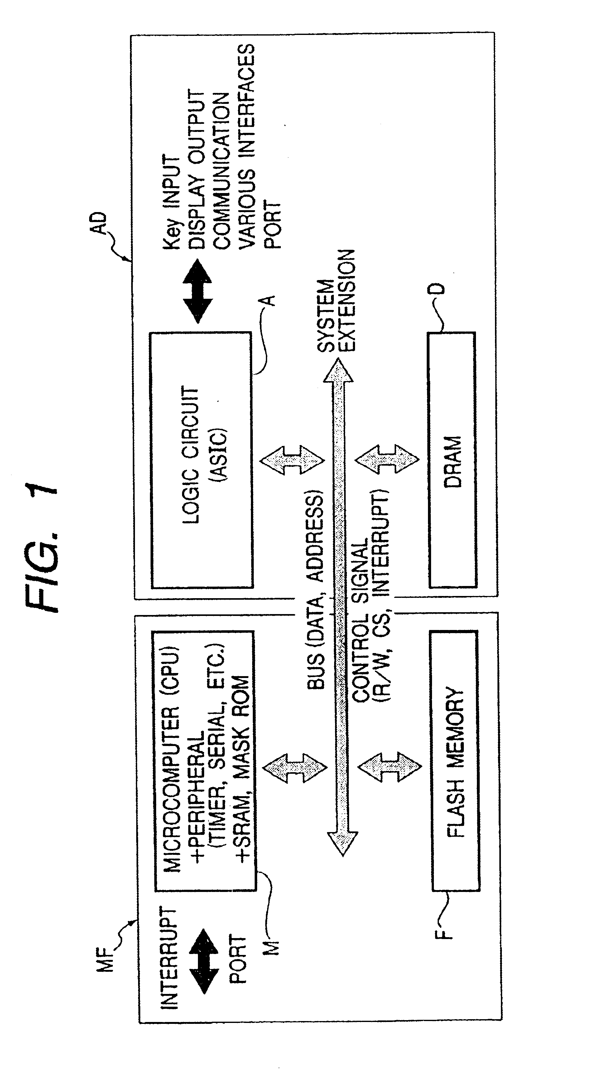
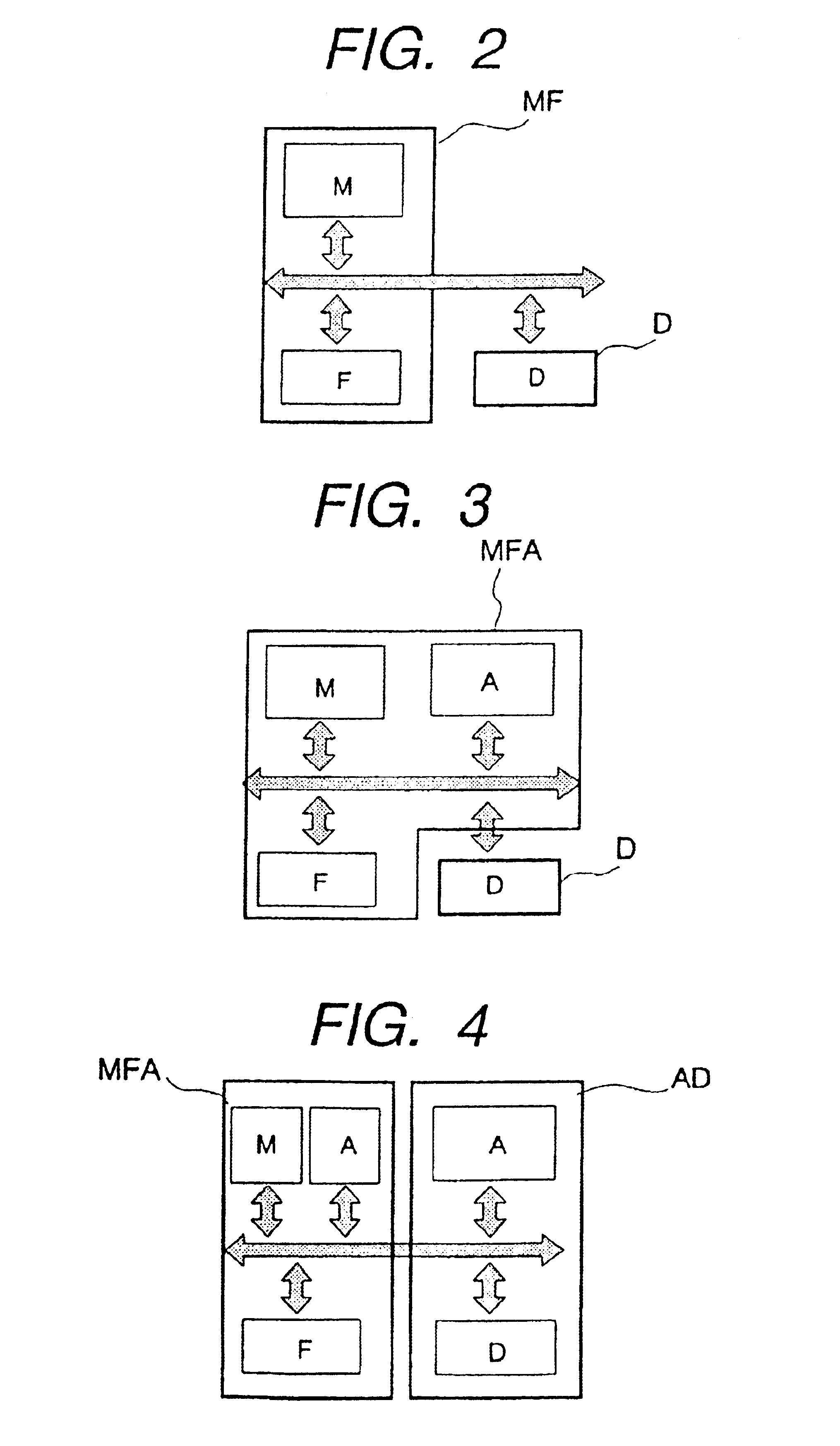
[0065]The semiconductor device according to the present embodiment is an LSI package having a stacked or multilayered structure in which a plurality of types of semiconductor chips are connected to one another so that signals can be inputted to and outputted therefrom. As shown in FIG. 1 as one example of its configuration, the semiconductor device comprises a chip MF (first semiconductor chip) referred to as a so-called flash memory-mounted microcomputer, which is equipped with a microcomputer M includi...


PUM


Abstract

Described herein is a stacked package according to the present invention, wherein a plurality of tape carriers which seal semiconductor chips, are multilayered in upward and downward directions. In the stacked package, one ends of leads formed over the whole surfaces of each tape carrier are electrically connected to their corresponding connecting terminals of the semiconductor chip. Other ends of the leads are electrically connected to their corresponding through holes defined in the tape carrier. Connecting terminals common to the plurality of semiconductor chips are formed at the same places of the plurality of tape carriers and withdrawn to the same external connecting terminals through a plurality of mutually-penetrated through holes.

Description

[0001]This is a continuation application of U.S. Ser. No. 10 / 050,950, filed Jan. 22, 2002, which is now U.S. Pat. No. 6,611,012; which is a continuation application of U.S. Ser. No. 09 / 984,089, filed on Oct. 26, 2001, now U.S. Pat. No. 6,492,719, which is a continuation application of U.S. Ser. No. 09 / 319,044, filed Jul. 30, 1999, now U.S. Pat. 6,335,565; which is a 371 of PCT / JP96 / 03549, filed Dec. 4, 1996. This application is related to U.S. Ser. No. 10 / 050,951, filed Jan. 22, 2002.TECHNICAL FIELD[0002]The present invention relates to a semiconductor device wherein a plurality of types of semiconductor chips are held in a single package from an MCM (Multi Chip Module)-based approach so that signals can be inputted thereto and outputted therefrom with respect to each other, and particularly to a technique effective for application to a semiconductor device wherein a microcomputer including a CPU (Central Processing Unit), a programmable non-volatile memory such as a flash memory or...

Claims


Application Information

Patent Timeline
IPC IPC(8): H01L23/495H01L23/498H01L23/48H01L25/10H01L27/108H10B12/00
CPCH01L23/49572H01L24/06H01L24/50H01L25/105H01L23/49816H01L25/0657H01L2225/107H01L27/10897H01L2224/0401H01L2224/04042H01L2224/06136H01L2224/48091H01L2224/48247H01L2924/01005H01L2924/01006H01L2924/01013H01L2924/01014H01L2924/01015H01L2924/01029H01L2924/0105H01L2924/01073H01L2924/01074H01L2924/01075H01L2924/01077H01L2924/01078H01L2924/01079H01L2924/01082H01L2924/01322H01L2924/014H01L2924/13091H01L2924/14H01L2924/1433H01L2924/15311H01L2924/15312H01L2924/15331H01L2924/19041H01L2924/3011H01L2225/1058H01L2225/1035H01L2225/1029H01L24/48H01L2924/01019H01L2924/01021H01L2924/01024H01L2924/01033H01L2924/01055H01L2224/16245H01L2924/3511H01L2924/00014H01L2224/451H01L2224/45144H01L2924/181H01L2924/12033H01L24/45H01L2224/48465H01L24/86H10B12/50H01L2924/00015H01L2224/05599H01L2924/00H01L2924/00012
Inventor MIYAMOTO, TOSHIONISHIMURA, ASAONOGUCHI, KOKIMICHISHITA, SATOSHIHORIGUCHI, MASASHIKUBO, MASAHARUSHIBA, KAZUYOSHI
Owner TESSERA ADVANCED TECH
Features
  • R&D
  • Intellectual Property
  • Life Sciences
  • Materials
  • Tech Scout
  • Unparalleled Data Quality
  • Higher Quality Content
  • 60% Fewer Hallucinations
Learn More