Mapping sensor system for detecting positions of flat objects

a sensor system and flat object technology, applied in the direction of optical detection, material analysis, instruments, etc., can solve the problems of reducing process yield, affecting the accuracy of detecting the position of flat objects, etc., to achieve reliable operation

Inactive Publication Date: 2005-05-31
MULTIMETRIXS
View PDF1 Cites 5 Cited by
  • Summary
  • Abstract
  • Description
  • Claims
  • Application Information

AI Technical Summary

Benefits of technology

[0022]It is an object of the present invention to provide a mapping sensor system for detecting, memorizing positions of flat objects, and controlling movements of the robot arm. Another object is to provide the mapping sensor system of the aforementioned type which is reliable in operation, not sensitive to false signals, distinctly differentiates between empty and occupied slots of wafer cassettes, operates irrespective of the position of a notch or flat on the periphery of the semiconductor wafer, detects double-stacked and inclined wafer in the cassette, can operate with low-power laser light sources and hence without the use of intensified light signals dangerous for operator's health. It is another object to provide a mapping sensor system of the aforementioned type, which operates with profiled light beams specifically modified for reflection from curvilinear peripheral edge of the wafer. Still another object is to provide a method for mapping flat objects located in slots of a cassette.
[0023]The mapping sensor system of the invention is intended for use with a mechanical arm of an industrial robot which loads and unloads flat circular objects, such as semiconductor wafers or glass substrates, into and from wafer cassettes on operations of processing the semiconductor wafers in stand-alone or cluster machines used in semiconductor production. The mapping system consists of a light source, a light-receiving unit, and a light beam shaper. The light source is installed on the front end of the robot arm and directs the light via the beam shaper to the leading edge of the semiconductor wafer. The beam reflected from the wafer edge is sensed by a light-receiving element, such as a photodiode receiver. The purpose of the shaper is to modify the shape and the cross-section of the beam directed towards the wafer so as to provide reflection from the curvilinear surface of the edge, irrespective of the existence of the notch or flat, most optimum for detection by the photodiode receivers and without generation of false signals, Another object is to increase the part of light reflected from the edge of the wafer. Still another purpose of the shaper is to transform a converging or pointed beam of high intensity into a spatially distributed beam of low intensity allowable for exposure to the operator. In one embodiment, the above objective is achieved by means of a special objective that contains a cylindrical lens. In another embodiment, the objective is achieved by utilizing an array of special microlenses which convert a single beam from a single light source into a plurality of beams modified in compliance with the point of incidence of the modified beams onto the wafer edge.

Problems solved by technology

However, sensing of the extremely thin, compoundly curved edges of semiconductor wafers has, until now, represented a significant challenge in developing edge sensing devices capable of rapidly and accurately sensing these edges.
However, the through-beam type sensors are difficult to align and, generally, must be dedicated to a cassette for specific parts.
Further, the through beam is unable to detect “double-stacking”; i.e., where two wafers or disks have inadvertently been mounted in the parts carrier so that their adjacent faces are in contact.
Double stacking invariably causes defects, such as scratches, on the precision surfaces of these products resulting in lower process yields and increased costs due to rejected parts.
Through-beam detection of parts will not be able to identify double-stacked or cross-slotted parts in those carriers where the parts are tilted or slightly askew in their slots.
Another process-related error, which may result in product defects, is “cross-slotting.” Cross slotting occurs when a semiconductor wafer or magnetic disk is positioned in the parts carrier such that one edge of the wafer or disk in contact with the carrier is in the wrong retaining slot in the carrier.
Thinner wafers having a compoundly curved edge will not reflect sufficient light directly back to the fiber cable and, therefore, the sensor will not detect the disk.
This unreliability could result in process throughput deterioration because the fiber optic sensor erroneously senses there are no more parts to process causing the process to stop.
In either case, such unreliability will require that an operator or technician be present to continually monitor production processes, thus negating the reasons for installing automated parts handling.
This scheme is further limiting since the close proximity and the 90° angle of incidence required by the device precludes rapid scanning across the length of the carrier for a rapid parts count.
However, the device of Bartunek et al. does not solve some other problems associated with the use of known mapping sensors.
One unsolved problem consists in generation of false signals, e.g., when the sensor generates a signal that the cassette slot is occupied, while it is free.
This problem is associated with the loss of a valuable and expensive time of a working cycle.
Another more serious problem occurs in generation of a signal stating that the cassette slot is free while it is occupied by another wafer.
Such false signal may cause serious damage to the equipment by inserting an expensive treated wafer into the occupied slot of the cassette.
This operation may result in a crush or even in more serious and expensive damage.
Another general problem in connection with the use of known mapping sensors consists in that, in order to provide reliable operation of the sensors, it is necessary to in crease the power of laser light sources to the level unacceptable for operation in open spaces where the exposed laser light becomes dangerous for the operator.
Increase in the power of laser light sources is associated not only with hazard to the operator's health but also with intensification of light reflected from the inner walls of the cassette, which results in generation of many false signal.
Some of these intensified false signals may reach or even exceed the level of sensitivity of the mapping sensor, which in this case generates a false signal.
A third problem consists in that practically all conventional mapping sensors used in the semiconductor production field operate with difractionally-limited light beams having transverse dimensions comparable with the width of a notch on a disk.
However, the mapping system of FIG. 1A with a single beam B′1 focused on the edge E′ will not produce a signal if the beam B′1 falls onto the notch N′.

Method used


Image

  • Mapping sensor system for detecting positions of flat objects
  • Mapping sensor system for detecting positions of flat objects
  • Mapping sensor system for detecting positions of flat objects

Examples


Embodiment Construction

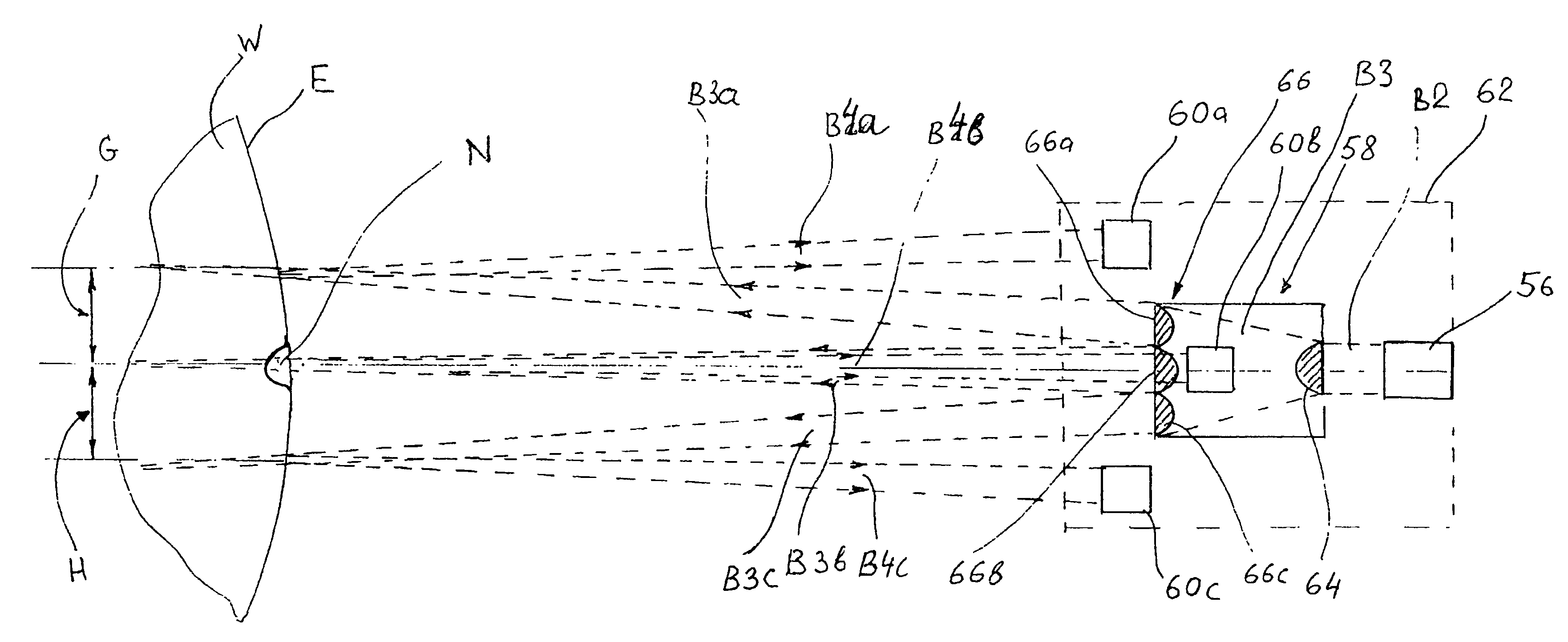
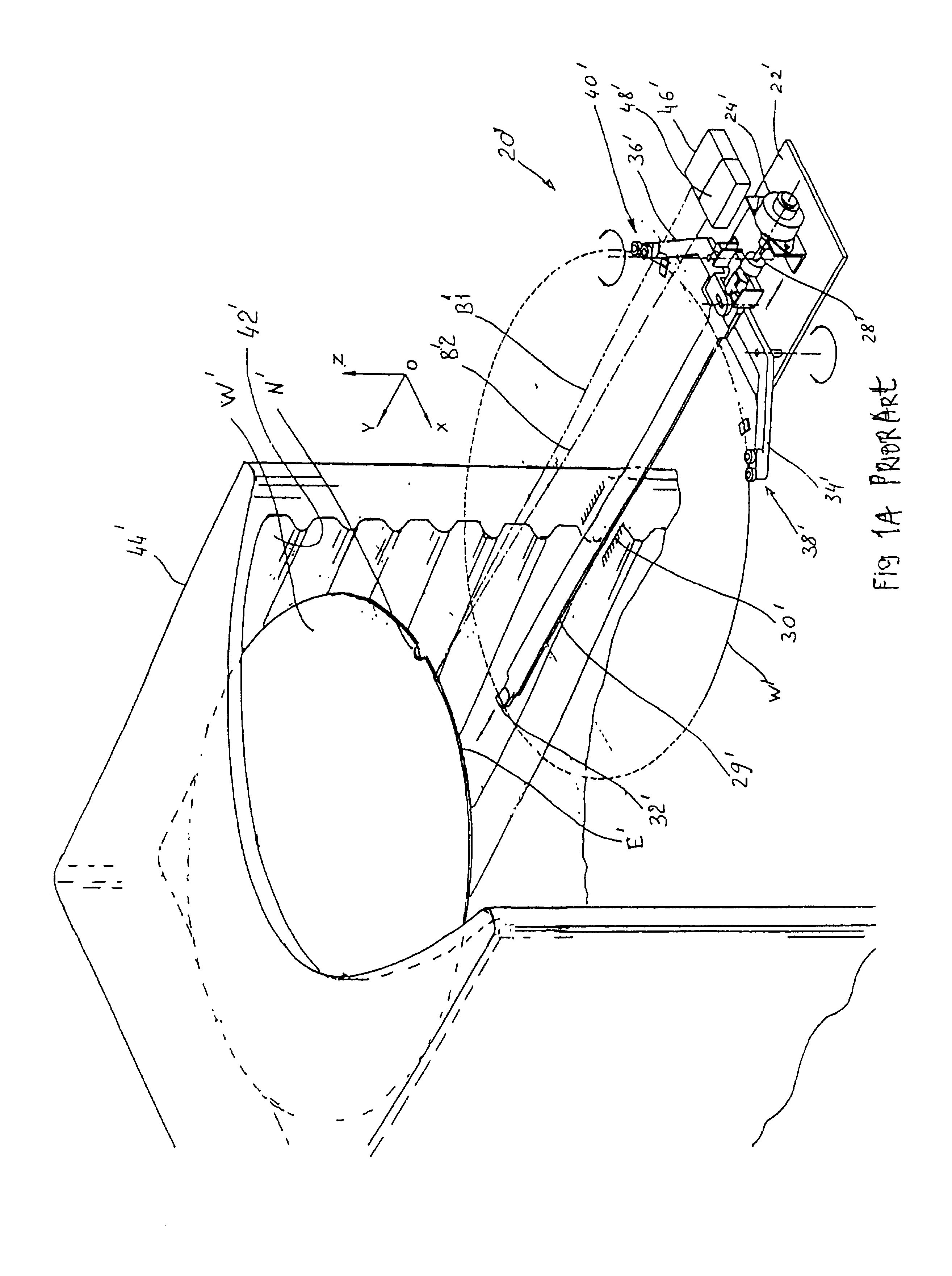
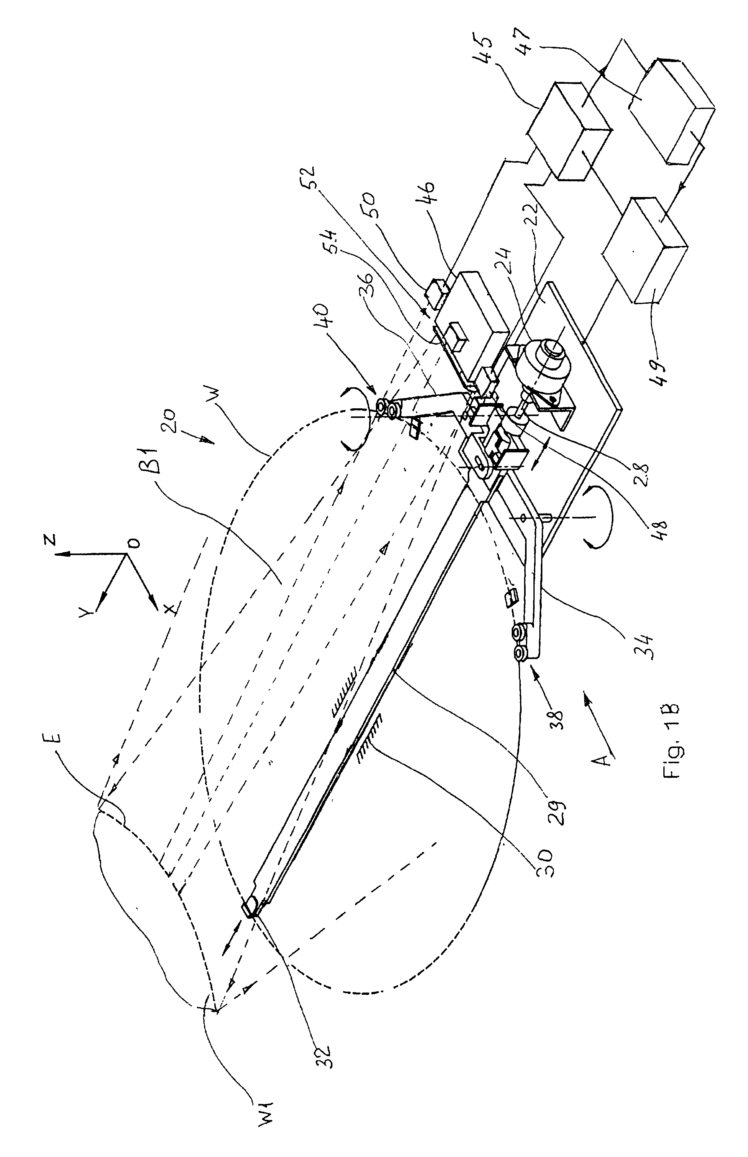
[0024]“The mapping sensor system of the present invention in conjuntion with a semiconductor wafer end effector, is shown in FIG. 1B which is a schematic three-dimensional view of the system” with the following—The mapping sensor system of the present invention in conjunction with an actuating mechanism, e.g., semiconductor wafer end effector, is shown in FIG. 1B which is a schematic three-dimensional view of the system.

[0025]The precision soft-touch gripping mechanism or end effector 20, which is used in conjunction with the mapping system of the invention has a mounting plate 22 attached to a robot arm (not shown). The plate 22 supports a stepper motor 24. The output shaft 28 of the stepper motor 24 is connected through a spring (not shown) to an elongated finger 29 that slides in a central longitudinal slot 30 of the plate 22 and supports a first wafer gripping post 32, pivotally supports two L-shaped fingers 34 and 36 with a second and third wafer gripping posts 38 and 40 on the...


PUM

PropertyMeasurementUnit
angleaaaaaaaaaa
angle of incidenceaaaaaaaaaa
thicknessaaaaaaaaaa

Abstract

The mapping sensor system of the invention is intended for use with a mechanical arm of an industrial robot which loads and unloads flat circular objects, such as semiconductor wafers, into and from wafer cassettes on operations of processing the semiconductor wafers in stand-alone or cluster machines used in semiconductor production. The mapping system consists of a light source, a light-receiving element, and a light beam shaper. The light source is installed on the front end of the robot arm and directs the light via the beam shaper to the leading edge of the semiconductor wafer. The beam reflected from the wafer edge is sensed by a light-receiving element, such as a photodiode. The shaper modifies the shape and the cross-section of the beam directed towards the wafer so as to provide reflection from the curvilinear surface of the edge, irrespective of the existence of the notch, most optimum for detection by the photodiodes and without generation of false signals. In one embodiment, the beam shaper contains a special objective with a cylindrical lens. In another embodiment, the beam shaper comprises an anamorphotic objective with an array of microlenses.

Description

FIELD OF THE INVENTION[0001]The present invention relates to a mapping sensor system for detecting positions of flat objects, in particular for mapping positions of semiconductor wafers in the slots of wafer cassettes, or the like. The mapping sensor system of the invention is intended for use in conjunction with operation of a mechanical arm of an industrial robot, in particular for loading / unloading semiconductor wafers to / from operation positions on semiconductor manufacturing machines.BACKGROUND OF THE INVENTION[0002]In semiconductor industry, treatment of semiconductor wafers is always accompanied by operations of transfer and positioning of such wafers between the storage devices, such as wafer cassettes, and working stations of processing machines.[0003]In the case of a stand-alone machine, manipulation with the wafers normally consists in transferring a wafer from one cassette to the stand-alone machine with the subsequent transfer of the treated wafer from the machine to an...

Claims


Application Information

Patent Timeline
Patent Type & Authority Patents(United States)
IPC IPC(8): G01V8/12
CPCG01V8/12
Inventor KESIL, BORISMARGULIS, DAVIDGERSHENZON, ELIK
Owner MULTIMETRIXS
Why Eureka
Try Eureka