Semiconductor chip capable of implementing wire bonding over active circuits

a technology of active circuits and semiconductors, applied in the field of semiconductor integrated circuits, can solve the problems of limited pad area of chips, impose constraints on wire bonding, and more costly choice to counteract this trend, and achieve the effect of saving valuable silicon area

Active Publication Date: 2005-05-31
UNITED MICROELECTRONICS CORP
View PDF8 Cites 68 Cited by
  • Summary
  • Abstract
  • Description
  • Claims
  • Application Information

AI Technical Summary

Benefits of technology

[0006]It is therefore the primary object of the present invention to provide an improved integrated circuit having a reinforced bonding pad structure capable of implementing BOAC, thereby saving valuable silicon area.

Problems solved by technology

For some devices, this results in chips that are pad area limited.
These lead to device designs with tighter bond pad sizes and pitches and consequently imposes constraints on wire bonding.
Choices to counteract this trend may be more costly area array interconnection solutions such as bumped chips for flip chip assembly.
As known to those skilled in the art, the prior art design rules exclude the area covered by the bonding pads from use for laying out actual circuit patterns because of the high risk of damaging the circuit structures due to the unavoidable forces needed in the bonding process.

Method used


Image

  • Semiconductor chip capable of implementing wire bonding over active circuits
  • Semiconductor chip capable of implementing wire bonding over active circuits
  • Semiconductor chip capable of implementing wire bonding over active circuits

Examples


Embodiment Construction

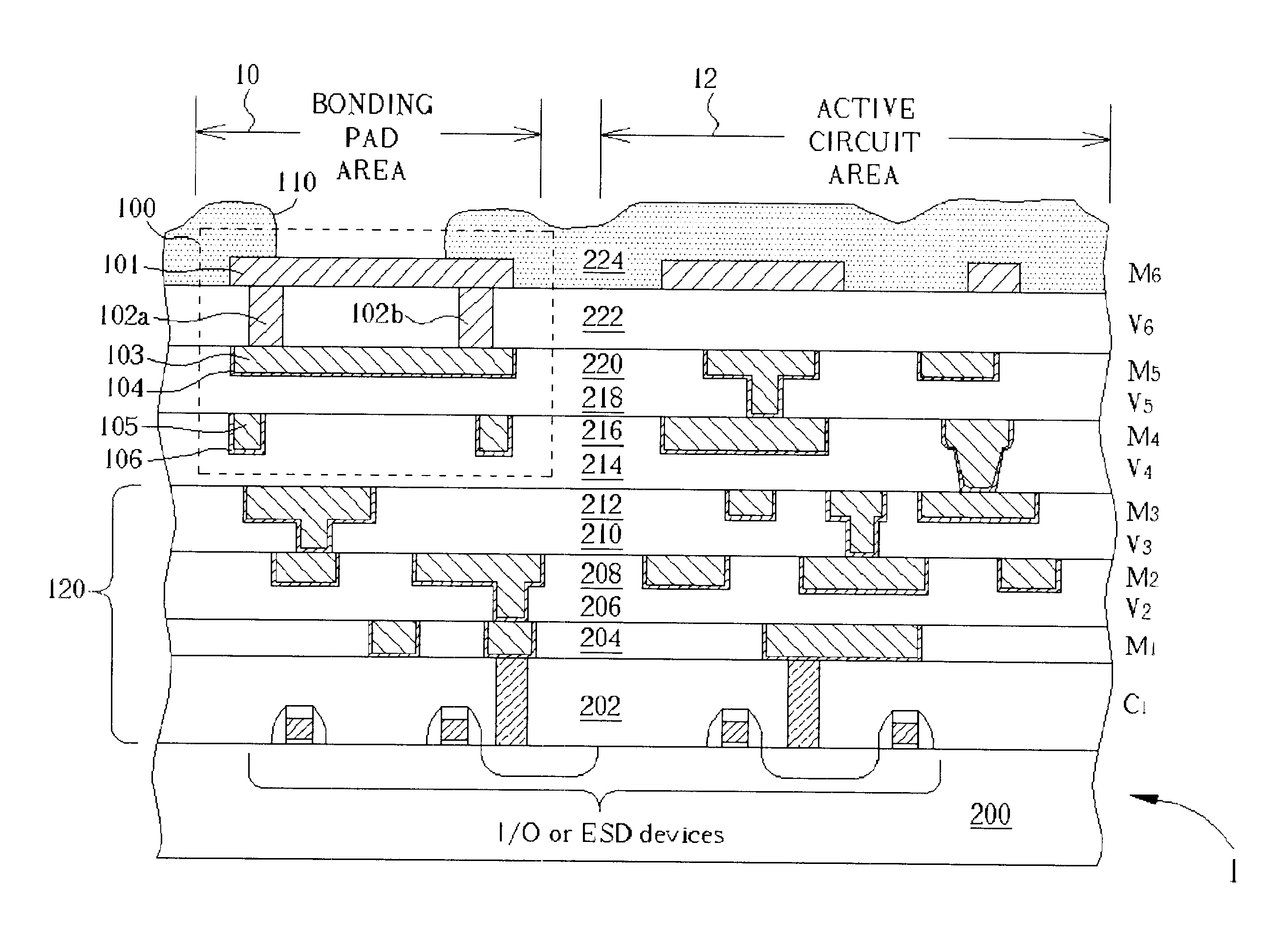
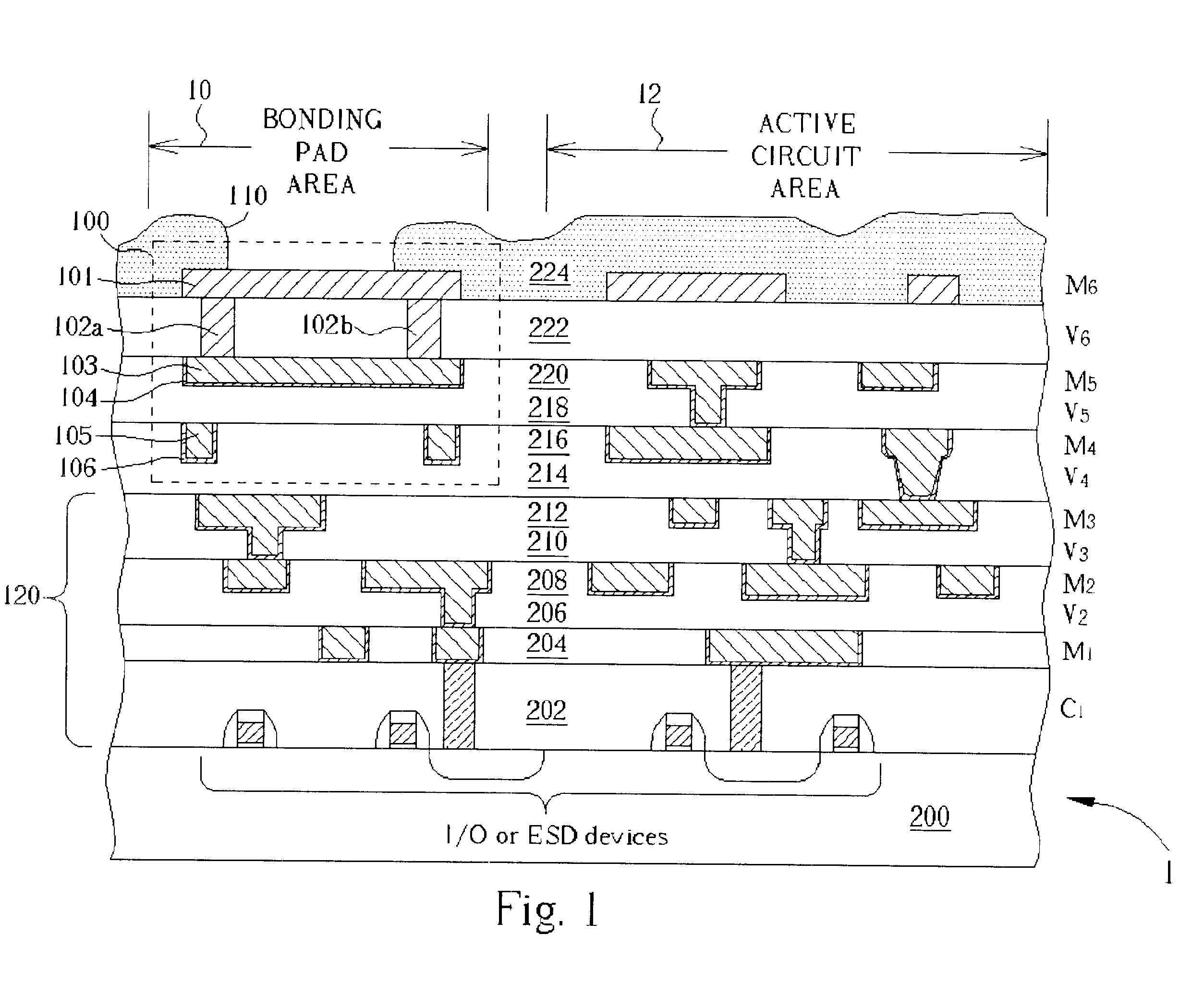
[0012]Please refer to FIG. 1. FIG. 1 is a schematic cross-sectional diagram illustrating pivotal portions of an exemplary integrated circuit capable of implementing BOAC in accordance with the first preferred embodiment of the present invention. As shown in FIG. 1, the integrated circuit 1 according to the present invention comprises a bonding pad area 10 and an active circuit area 12. A bonding pad reinforcement structure 100 is disposed within the bonding pad area 10. Portions of the active circuit components 120 of the integrated circuit 1 are situated directly under the bonding pad reinforcement structure 100. By way of example, the active circuit components may include input / output (I / O) devices / circuits, or Electrostatic Discharge (ESD) devices / circuits, each of which may further consist of a plurality of semiconductor devices, which are fabricated on a main surface of a substrate 200, for example, such as metal-oxide-semiconductor field-effect transistors (MOSFETs), ion diffu...


PUM

PropertyMeasurementUnit
mechanical stressaaaaaaaaaa
surface areaaaaaaaaaaa
stress-aaaaaaaaaa

Abstract

An integrated circuit including a reinforced bonding pad structure is disclosed. The reinforced bonding pad structure includes a bondable metal layer defined on a stress-buffering dielectric layer, and an intermediate metal layer damascened in a first inter-metal dielectric (IMD) layer disposed under the stress-buffering dielectric layer. The intermediate metal layer is situated directly under the bondable metal layer and is electrically connected to the bondable metal layer with a plurality of via plugs integrated with the bondable metal layer. At least one metal frame is damascened in a second IMD layer under the first IMD layer. The metal frame is situated directly under the intermediate metal layer for counteracting mechanical stress exerted on the bondable metal layer during bonding. An active circuit portion including active circuit components of the integrated circuit is situated directly under the metal frame of the reinforced bonding pad structure.

Description

BACKGROUND OF INVENTION[0001]1. Field of the Invention[0002]The present invention relates to the field of semiconductor integrated circuits (ICs), and more particularly to a semiconductor chip capable of employing wire bonding over active circuits (also referred to as “BOAC”).[0003]2. Description of the Prior Art[0004]Technology improvements continue to drive the evolution of integrated circuits toward increased complexity and smaller feature sizes. At the same time, chips are being designed for wider word systems that require larger numbers of input / output (I / O) connections. For some devices, this results in chips that are pad area limited. That is, the peripheral area required by the bonding pads defines the chip size rather than the smaller area required by the active circuits. These lead to device designs with tighter bond pad sizes and pitches and consequently imposes constraints on wire bonding. Choices to counteract this trend may be more costly area array interconnection sol...

Claims


Application Information

Patent Timeline
Patent Type & Authority Patents(United States)
IPC IPC(8): H01L23/485H01L23/48
CPCH01L24/05H01L2224/02166H01L2224/05095H01L2224/05624H01L2924/01005H01L2924/01006H01L2924/01013H01L2924/01014H01L2924/01022H01L2924/01029H01L2924/0105H01L2924/01073H01L2924/01082H01L2924/014H01L2924/04941H01L2924/05042H01L2924/13091H01L2924/14H01L2924/19041H01L2224/05093H01L2924/01033H01L2924/01019
Inventor WANG, KUN-CHIHWU, BING-CHANG
Owner UNITED MICROELECTRONICS CORP
Why Eureka
Try Eureka