Liquid crystal electrooptical device

Inactive Publication Date: 2005-05-31
SEMICON ENERGY LAB CO LTD
View PDF22 Cites 34 Cited by
  • Summary
  • Abstract
  • Description
  • Claims
  • Application Information

AI Technical Summary

Benefits of technology

[0026]In addition thereto, the present invention particularly discloses means for connecting lead wirings of a panel array substrate with lead wirings of a stick substrate with high accuracy and it is an object of the present invention to provide an electrooptical device having high yield and excellent display characteristic.

Problems solved by technology

However, in the case of CRT volume, weight and power consumption of the device are large and particularly, CRT is not suitable for a display device having a large area.
Particularly, in the case of a display device having a large area, a number of the electrode wirings is further increased and accordingly, there poses a problem in which a number of ICs is increased resulting in an increase in cost.
However, in the case where the panel portion and the drive portion are integrally formed on the same substrate, when heat or force from outside is effected, warp or the like is caused in the entire substrate and adverse influence is effected on a peripheral drive circuit installed on the same substrate by a substrate interval control member (spacer or the like).
As a result, the peripheral drive circuit is not normally operated and deterioration in reliability and durability of a liquid crystal electrooptical device is caused.
Further, the panel portion and the drive portion are simultaneously formed and accordingly, the yield is deteriorated particularly in the case of a display device having a large area.
However, it becomes necessary to carry out a processing for a long period of time at high temperature of 600° C. or higher as heating temperature and accordingly, there poses a problem in which the substrate is irreversibly shrunk.
When an electrooptical device is fabricated by adhering the panel array substrate formed by the amorphous silicon semiconductor as a semiconductor material of TFTs in this way, with the stick substrate formed by the silicon semiconductor having the crystalline performance as a semiconductor material of TFTs, the following problem is caused.
The panel array substrate uses the amorphous silicon semiconductor and therefore, almost no shrinkage is caused in the substrate (shrinkage of substrate), however, the stick substrate has been subjected to a thermal treatment at high temperatures to provide the silicon semiconductor having the crystalline performance and therefore, shrinkage is caused.
Further, in the steps of connecting the panel array substrate and the stick substrate of (3), the wiring patterns may slightly be shifted from each other in the connecting operation and there also poses a problem in which connection failure is enhanced and reliability is deteriorated by the positional shift in the wiring patterns in this case.

Method used


Image

  • Liquid crystal electrooptical device
  • Liquid crystal electrooptical device
  • Liquid crystal electrooptical device

Examples


embodiment 1

[0081](Embodiment 1)

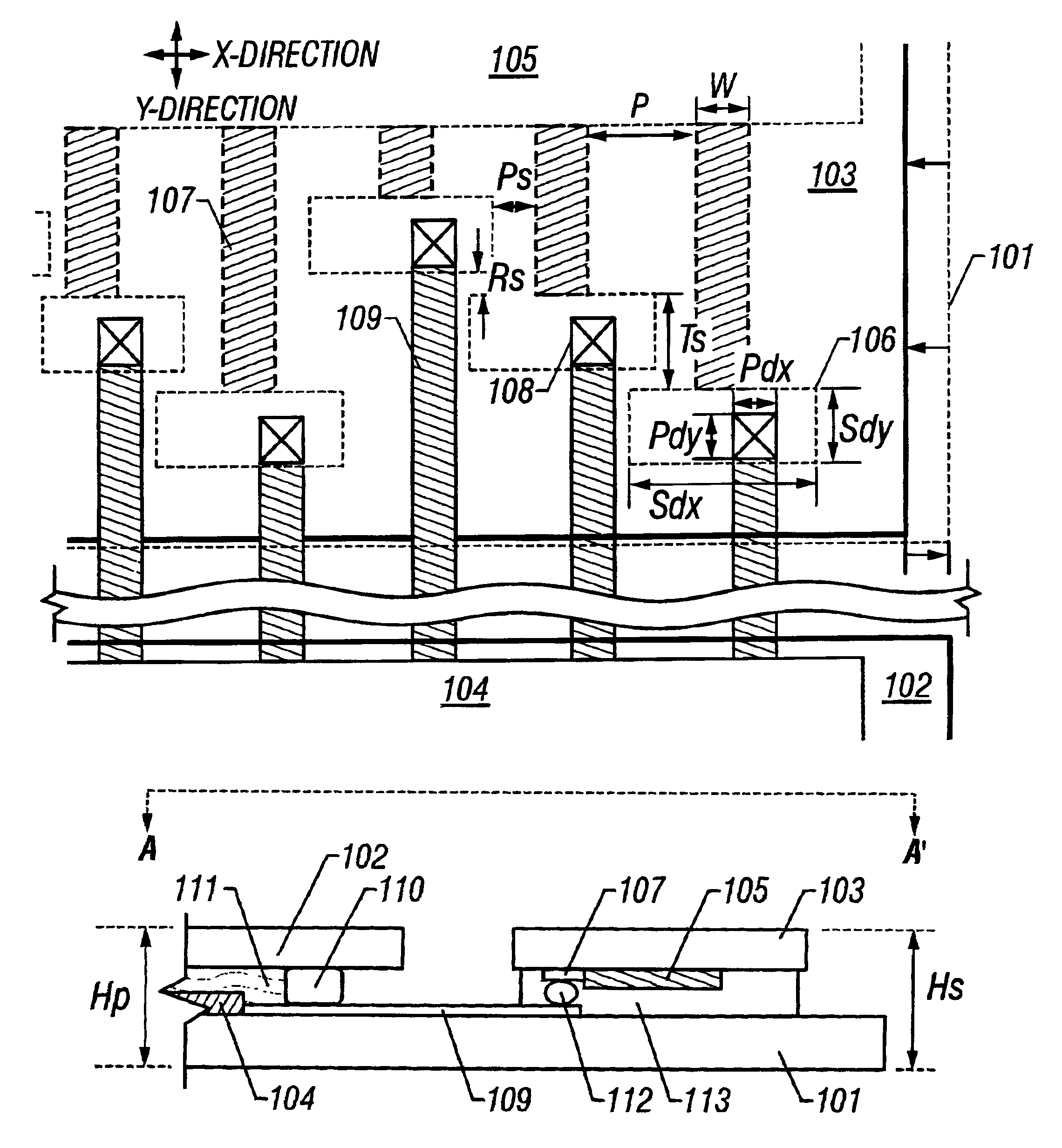
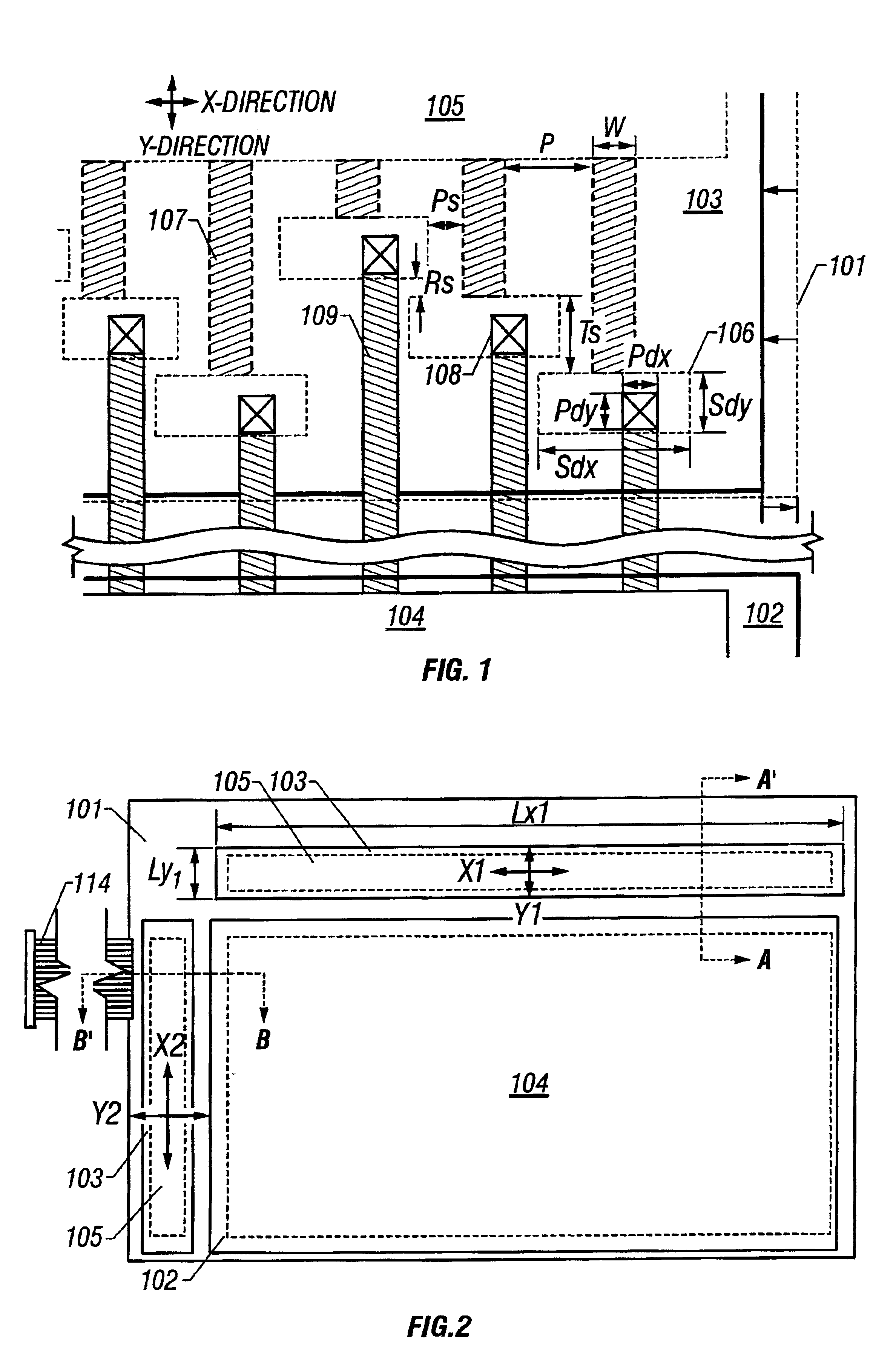
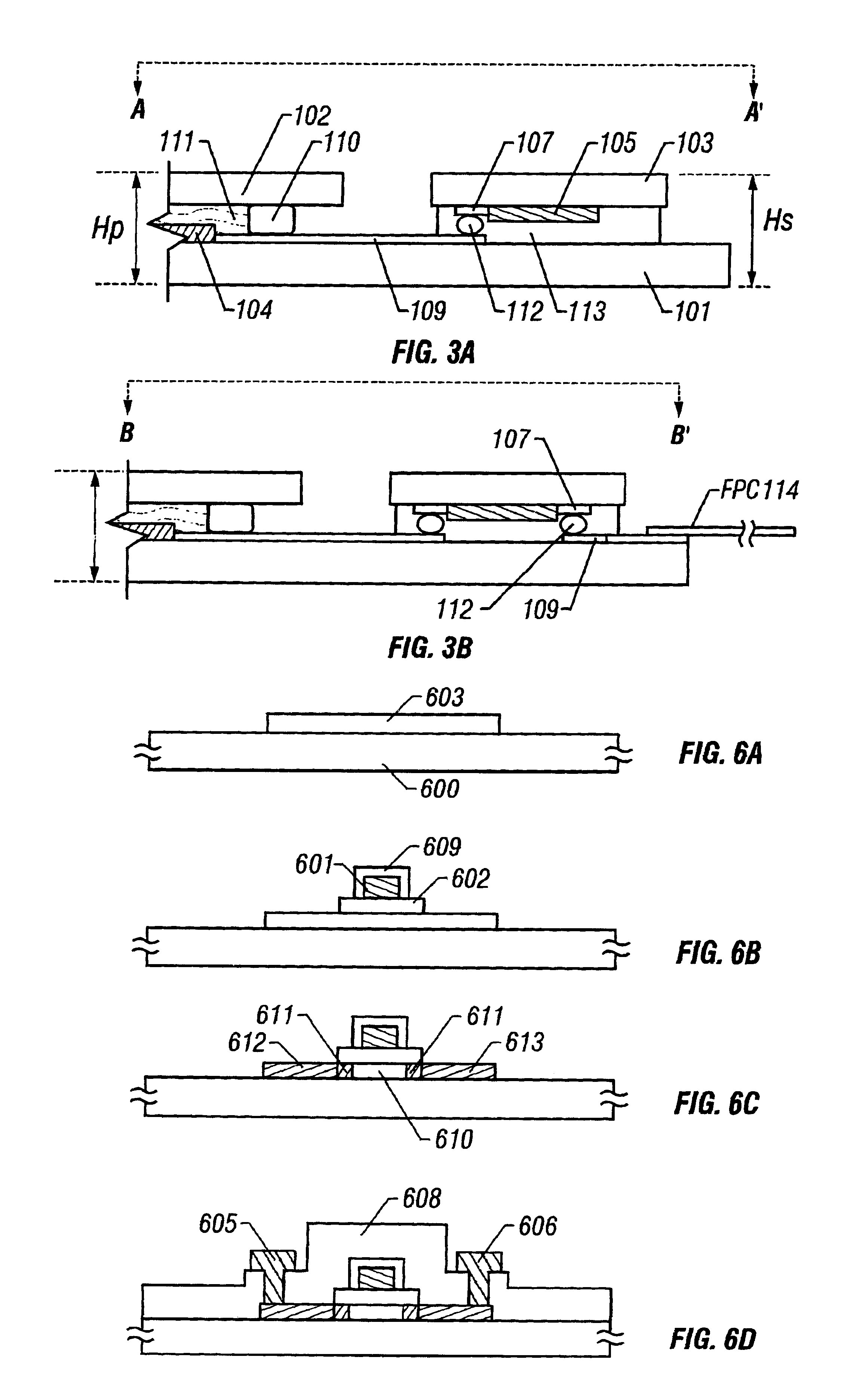
[0082]The embodiment shows an outline of steps of fabricating a panel, steps of fabricating a stick substrate and steps of connecting the panel array substrate and the stick substrate. An explanation will be given of the embodiment in reference to FIGS. 1, 2, 3(a), 3(b), 4(A), 4(B), 4(C), 4(D), 5, 6(A), 6(B), 6(C) and 6(D). FIG. 2 is a simplified view of a total of an electrooptical device according to the present invention. Further, FIGS. 3(a) and 3(b) are a sectional view taken along a line A-A′ of FIG. 2 and a sectional view taken along a line B-B′ thereof.

[0083](Fabrication steps of panel)

[0084]In this embodiment, there is constituted a switching element used in a pixel matrix on a panel array substrate 400 by using amorphous silicon semiconductor which is used most generally since the fabrication temperature is low and the element can be fabricated comparatively easily by a gas phase process and is excellent in mass production performance.

[0085]As a structur...

embodiment 2

[0121](Embodiment 2)

[0122]FIG. 7 shows an outline view of a total of a device according to the embodiment.

[0123]In respect of a method of fabricating the device, a device can be fabricated by steps the same as those in Embodiment 1. Although Embodiment 1 is provided with a constitution in which two sheets of the stick substrates are used, in this embodiment, an example in which three sheets of the stick substrates are used is shown. Also, further integration is carried out by installing two sheets of VLSI (Very Large Scale Integrated Circuit) substrates 706 mounted with a control circuit, a memory circuit and so on. The VLSI substrate is constituted to use a silicon substrate. In respect of the VLSI substrate, one sheet, two sheets or a number of sheets of more than two thereof may be used.

[0124]Numeral 701 designates a panel array substrate, numeral 702 designates an opposed substrate, numeral 703 designates a stick substrate, numeral 704 designates a region of forming a pixel matr...


PUM


Abstract

To provide means for resolving a problem in which in steps of connecting a panel array substrate and a stick substrate, connection failure is enhanced and reliability is deteriorated by a positional shift caused in connecting operation and a positional shift caused by shrinkage of the substrate, a shape of a total of a stick substrate 103 is constituted by a rectangular shape (lx1×ly1) and contiguous electrode pads are annaged to shirt by Ts in Y-direction by which lead wirings of the panel array substrate and lead wirings of the stick substrate can be connected with high accuracy and an electrooptical device having high yield and excellent display characteristic is provided.

Description

CROSS-REFERENCE TO RELATED APPLICATIONS[0001]This application is a divisional application of and claims priority to U.S. application Ser. No. 09 / 198,073 filed Nov. 23, 1998 now U.S. Pat. No. 6,362,866.BACKGROUND OF THE INVENTION[0002]1. Field of the Invention[0003]The present invention relates to a liquid crystal electrooptical device using a display member of liquid crystal or the like, particularly to a constitution thereof.[0004]2. Description of Related Art[0005]The most general conventional display device is CRT (Cathode Ray Tube). However, in the case of CRT volume, weight and power consumption of the device are large and particularly, CRT is not suitable for a display device having a large area. Hence, in recent years, a liquid crystal electrooptical device capable of realizing light weight formation and low power consumption formation more easily than CRT attracts attention.[0006]According to a liquid crystal electrooptical device, a difference in the dielectric constant of ...

Claims


Application Information

Patent Timeline
IPC IPC(8): G02F1/13G02F1/1343G02F1/136G02F1/1368H01L29/786
CPCG02F1/13452G02F1/1345
Inventor YAMAZAKI, SHUNPEIKOYAMA, JUN
Owner SEMICON ENERGY LAB CO LTD
Why Eureka
Try Eureka