Method and apparatus for electro-chemical mechanical deposition

a mechanical deposition and electrochemical technology, applied in the direction of manufacturing tools, lapping machines, printing, etc., can solve the problems of high cost and defect density of developing and integrating local interconnections, copper thin film deposition into deep submicron via holes and trenches is becoming more difficult in ulsi chip processing, and the vias do not have the desired conductive characteristics, so as to prevent the accumulation of conductive materials and reduce the formation of electrolyte contact

Inactive Publication Date: 2005-06-07
NOVELLUS SYSTEMS
View PDF21 Cites 73 Cited by
  • Summary
  • Abstract
  • Description
  • Claims
  • Application Information

AI Technical Summary

Benefits of technology

[0014]These and other object of the present invention are obtained by depositing a conductive material form an electrolyte solution to a predetermined area of a wafer. The steps that are used when making this application include applying the conductive material to the predetermined area of the wafer using an electrolyte solution

Problems solved by technology

Conformal thin film deposition of copper into deep submicron via holes and trenches is becoming more difficult in ULSI chip processing, especially when the feature sizes are decreasing below the 0.25 μm with aspect rations of greater that 5 to 1.
These processes so far have yielded a very high cost and defect density for developing and integrating local interconnects for ULSI technology.
This prevention, however, is achieved at the expense of adding contaminants to the electrolytic solution, which results, in part, in vias that do not have the desired conductive characteristics.
In particular, the grain size of the deposited conductor, due to the use

Method used


Image

  • Method and apparatus for electro-chemical mechanical deposition
  • Method and apparatus for electro-chemical mechanical deposition
  • Method and apparatus for electro-chemical mechanical deposition

Examples


Embodiment Construction

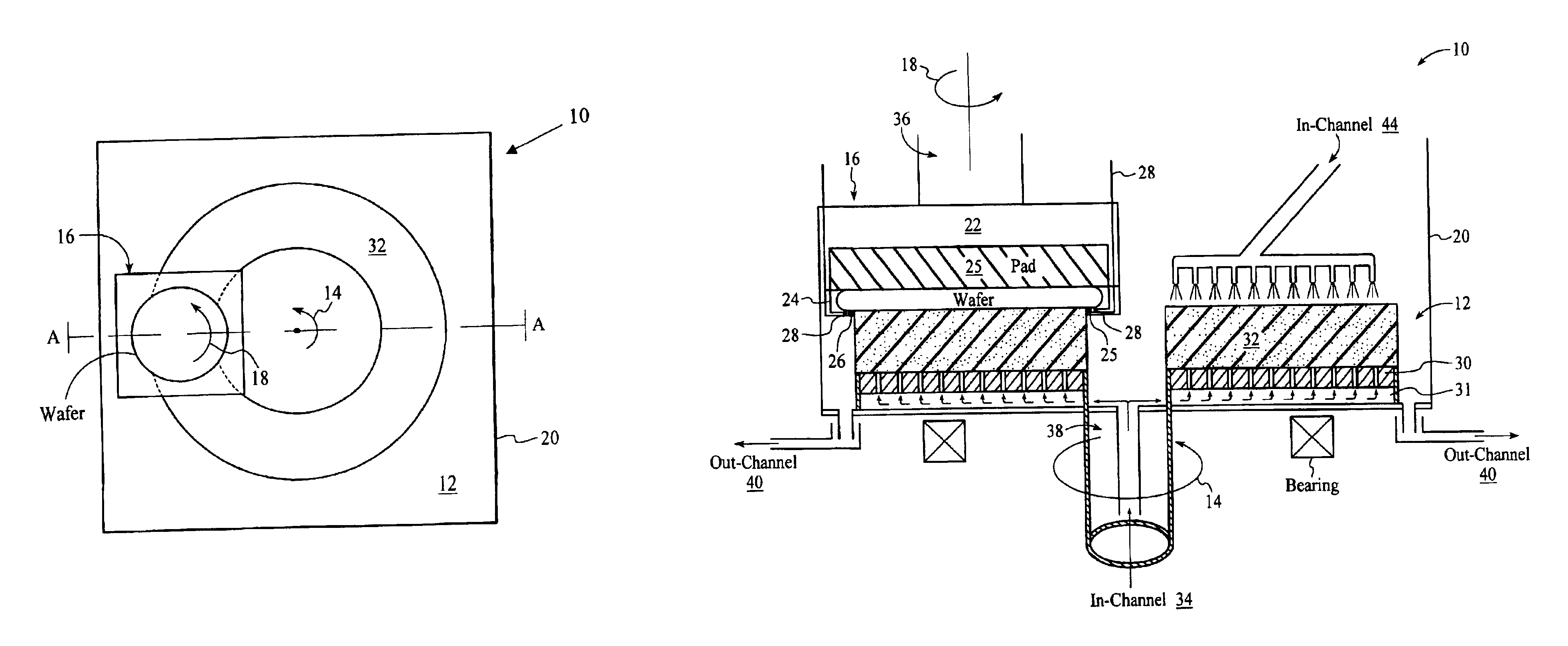
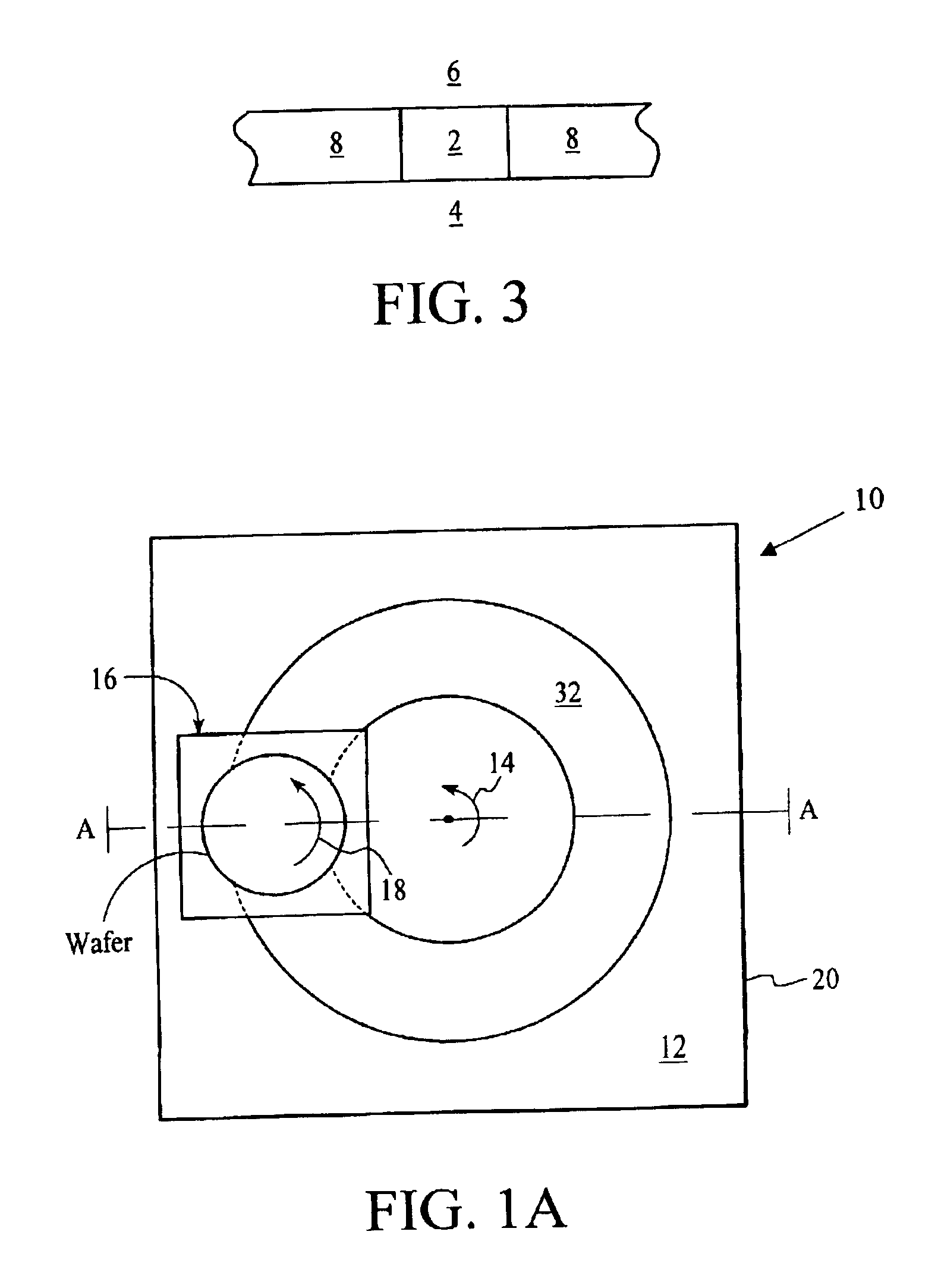
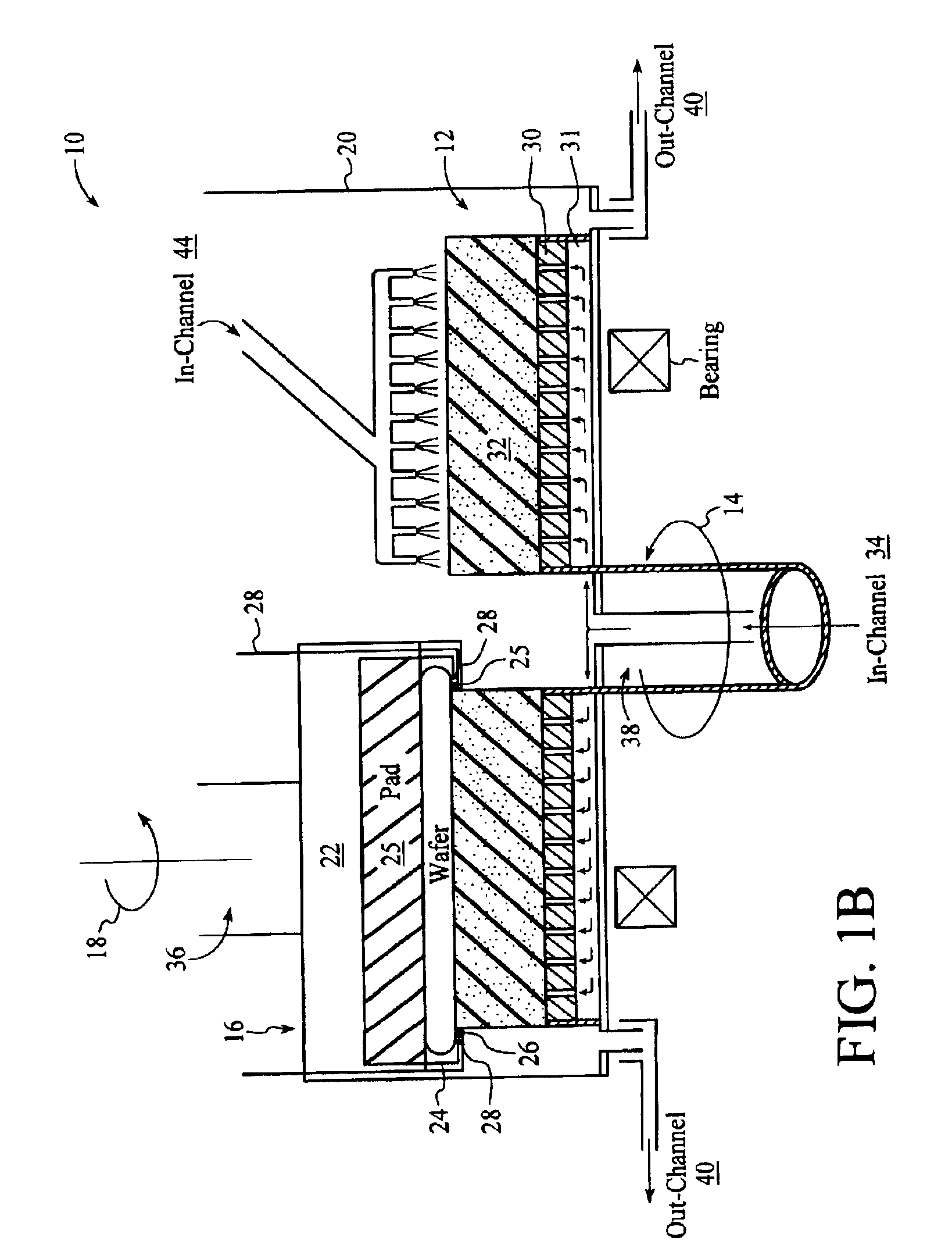
[0021]The preferred embodiments of the present invention will now be described. As noted above, conventional processing uses different equipment, at different times, in order to obtain conductive material within vias or at other desired locations on the surface of a semiconductor wafer that contains many different semiconductor chips, but not have the conductive material disposed at undesired locations. Accordingly, the equipment cost needed to manufacture a high quality semiconductor integrated circuit device can be exorbitant.

[0022]The present invention contemplates different embodiments which allow for the same device, termed a “electro chemical mechanical deposition apparatus”, to be used to both deposit a conductive material as well as then polish or reduce the rate of deposition of that conductive material. The “electro chemical mechanical deposition apparatus” can also be used to simultaneously deposit and / or polish the conductive material. While the present invention can be ...


PUM

PropertyMeasurementUnit
Polarityaaaaaaaaaa
Currentaaaaaaaaaa
Electrical conductoraaaaaaaaaa

Abstract

The present invention deposits a conductive material from an electrolyte solution to a predetermined area of a wafer. The steps that are used when making this application include applying the conductive material to the predetermined area of the wafer using an electrolyte solution disposed on a surface of the wafer, when the wafer is disposed between a cathode and an anode, and preventing accumulation of the conductive material to areas other than the predetermine area by mechanically polishing the other areas while the conductive material is being applied.

Description

RELATED APPLICATIONS[0001]This is a continuation of U.S. Ser. No. 09 / 607,567 filed Jun. 29, 2000, now U.S. Pat. No. 6,676,822, which is a divisional of U.S. Ser. No. 09 / 201,929 filed Dec. 1, 1998, now U.S. Pat. No. 6,176,992, incorporated herein by reference.BACKGROUND OF THE INVENTION[0002]1. Field of the Invention[0003]The present invention relates to a Method and Apparatus for Electro Chemical Mechanical Deposition, and more particularly, to a method and apparatus that provides for both the deposition and polishing of a conductive material on a semiconductor wafer.[0004]2. Background of the Invention[0005]Metallization of semiconductor wafers, i.e. deposition of a layer of metal on the face of wafers over a barrier / seed layer of metal has important and broad application in the semiconductor industry. Conventionally, aluminum and other metals are deposited as one of many metal layers that make up a semiconductor chip. More recently, there is great interest in the deposition of cop...

Claims


Application Information

Patent Timeline
IPC IPC(8): B24B37/04C25D5/02C25D5/06C25D5/22C25D5/00H01L21/288H01L21/02H01L21/321
CPCB24B37/20C25D5/02H01L21/3212C25D5/22H01L21/2885C25D5/06C25D5/627C25D5/617C25D5/611
Inventor TALIEH, HOMAYOUN
Owner NOVELLUS SYSTEMS
Why Eureka
Try Eureka