Method of fabricating a high performance MOSFET device featuring formation of an elevated source/drain region

a technology of mosfet and source/drain region, which is applied in the direction of semiconductor devices, basic electric elements, electrical apparatus, etc., can solve the problems of source/drain resistance, process difficulties, and difficulty in maintaining shallow source/drain regions, and achieve the effect of reducing the receding of the conductive gate structur

Inactive Publication Date: 2005-06-07
TAIWAN SEMICON MFG CO LTD
View PDF16 Cites 24 Cited by
  • Summary
  • Abstract
  • Description
  • Claims
  • Application Information

AI Technical Summary

Problems solved by technology

However it is difficult to maintain shallow source / drain regions during subsequent silicide procedures used to reduce source / drain resistance.
The thicker the silicide formation the greater the consumption of source / drain region, therefore presenting process difficulties when attempting to form silicide on the shallow source / drain regions needed for sub-50 nm MOSFET devices.
The removal of the insulator spacer component can however damage the exposed shallow source / drain region.
In addition some raised source / drain fabrication procedures do not allow silicide formation to occur on the gate structure, therefore limiting gate resistance reduction.

Method used


Image

  • Method of fabricating a high performance MOSFET device featuring formation of an elevated source/drain region
  • Method of fabricating a high performance MOSFET device featuring formation of an elevated source/drain region
  • Method of fabricating a high performance MOSFET device featuring formation of an elevated source/drain region

Examples


Embodiment Construction

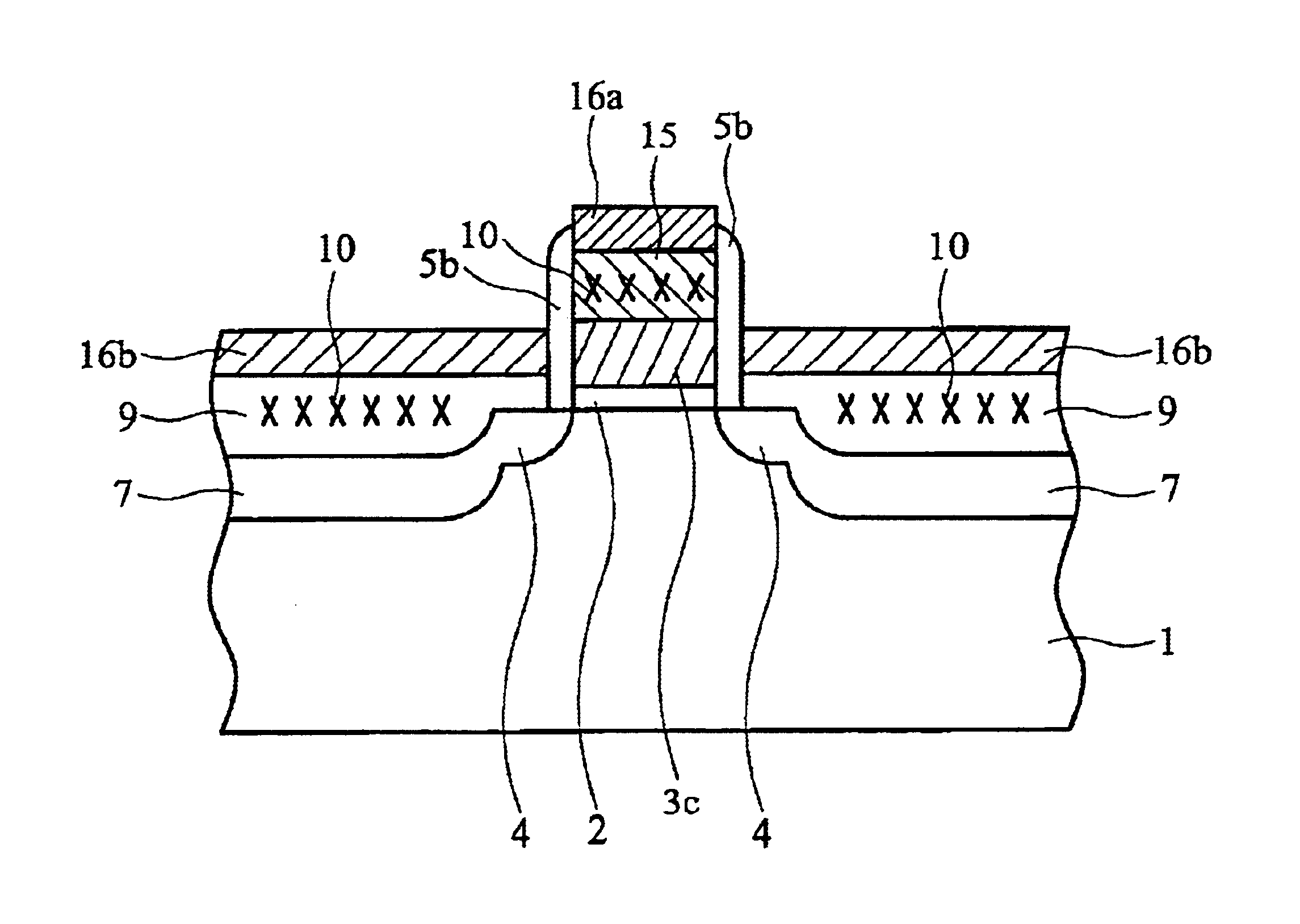
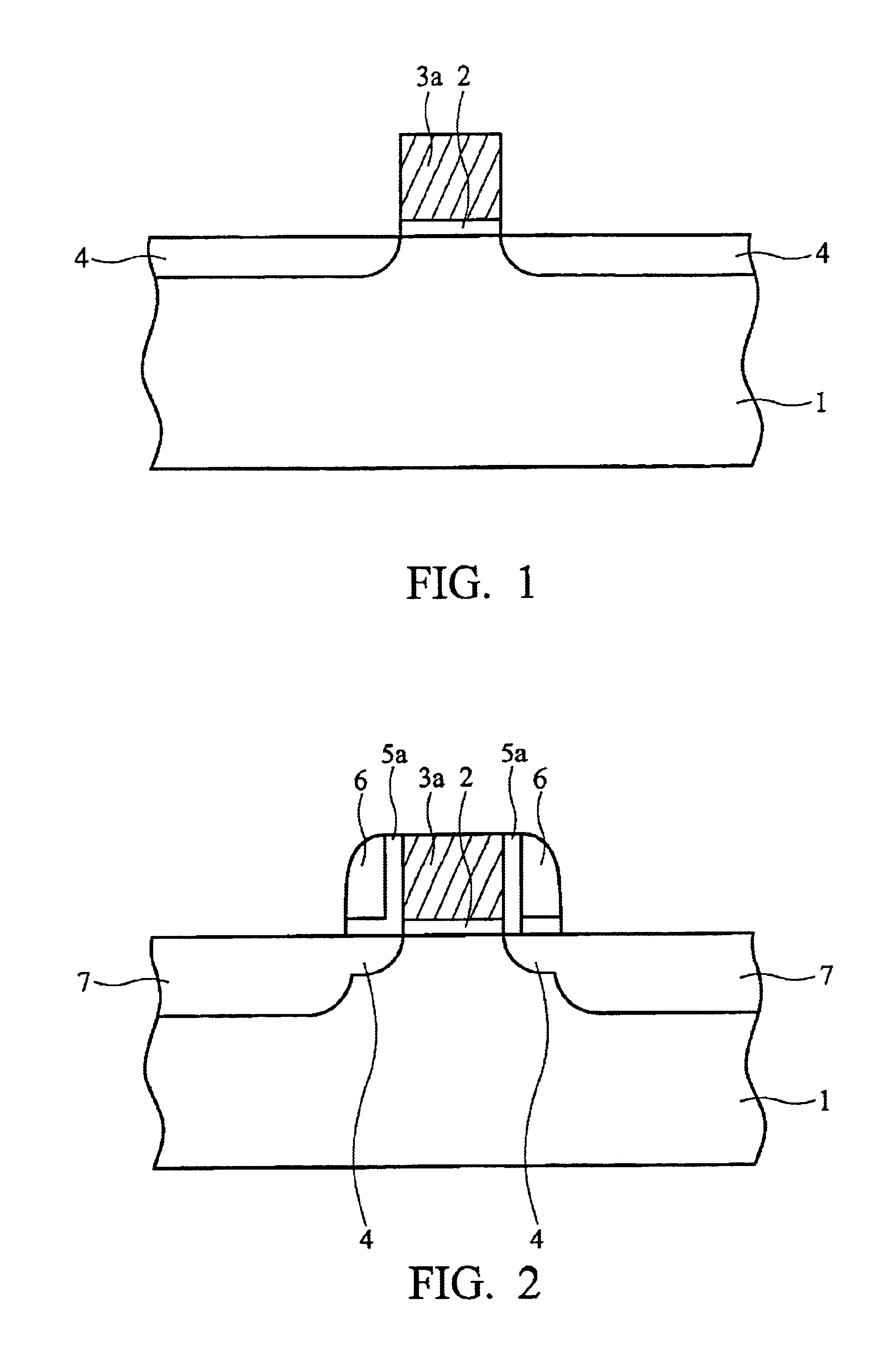
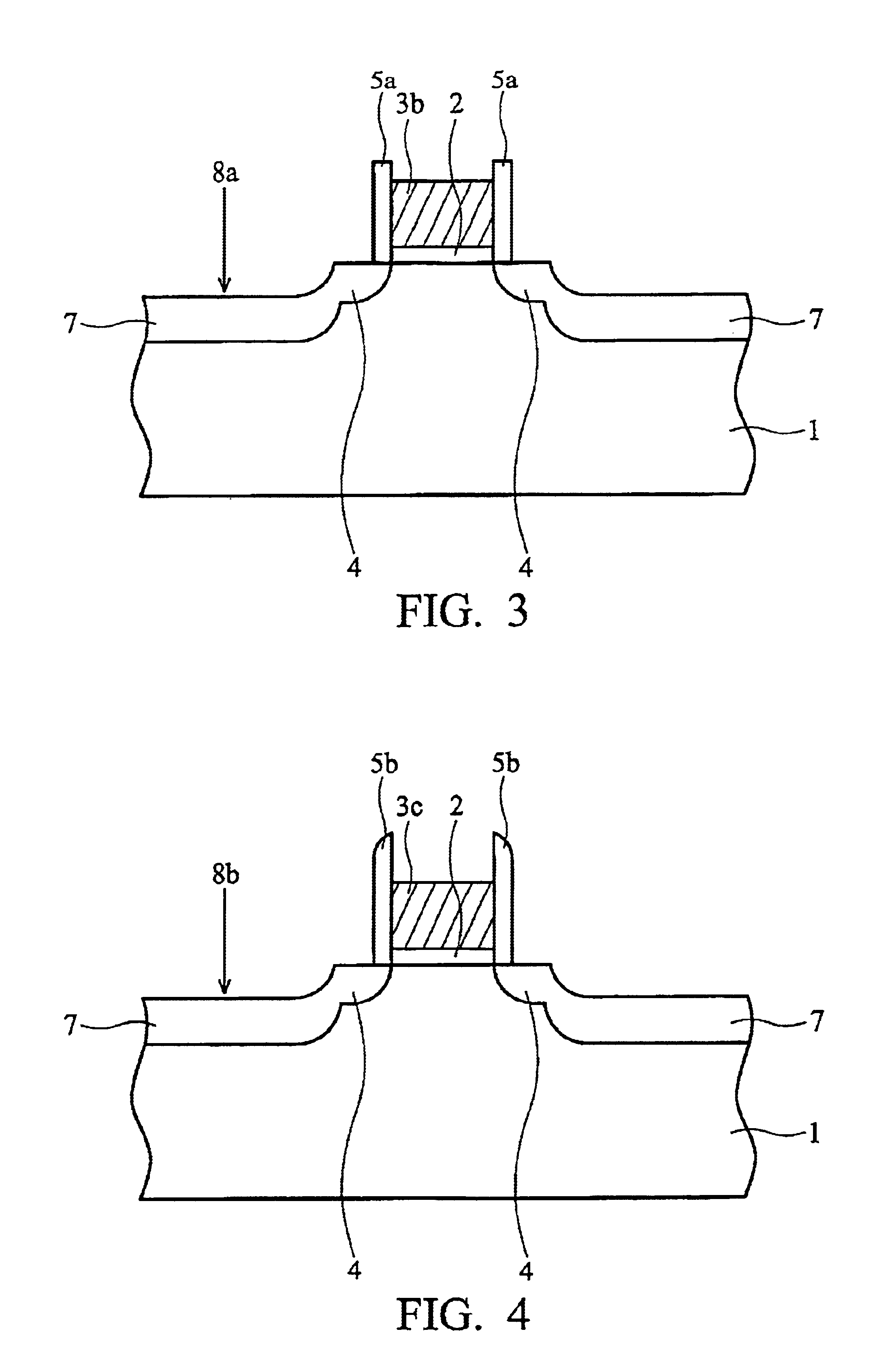
[0013]The method of fabricating a MOSFET device featuring a raised source / drain structure on a heavily doped source / drain region, and on a portion of lightly doped source / drain region, located in portion of a semiconductor substrate previously damaged during procedures used to remove components of a composite insulator spacer, will now be described in detail. Semiconductor substrate 1, comprised of single crystalline P type silicon, featuring a crystallographic orientation, is used and schematically shown in FIG. 1. Gate insulator layer 2, comprised of silicon dioxide, is thermally grown to a thickness between about 10 to 100 Angstroms, in an oxygen-steam ambient. A conductive material, such as polysilicon, is next deposited via low pressure chemical vapor deposition (LPCVD), procedures, to a thickness between about 500 to 3000 Angstroms. The polysilicon layer can be doped in situ during deposition via the addition of arsine, or phosphine to a silane or disilane ambient, or the pol...


PUM


Abstract

A method of fabricating a MOSFET device featuring a raised source / drain structure on a heavily doped source / drain region as well as on a portion of a lightly doped source / drain (LDD), region, after removal of an insulator spacer component, has been developed. After formation of an LDD region a composite insulator spacer, comprised of an underlying silicon oxide spacer component and an overlying silicon nitride spacer component, is formed on the sides of a gate structure. Formation of a heavily doped source / drain is followed by removal of the silicon nitride spacer resulting in recessing of, and damage formation to, the heavily doped source / drain region, as well as recessing of the gate structure. Removal of a horizontal component of the silicon oxide spacer component results in additional recessing of the heavily doped source / drain region, and of the gate structure. A selective epitaxial growth procedure is then used to form a raised, single crystalline silicon structure on the recessed and damaged heavily doped source / drain and LDD regions, while a polycrystalline silicon structure is grown on the underlying recessed gate structure. Metal silicide is then formed on the raised, single crystalline silicon structure and on the polycrystalline silicon structure.

Description

BACKGROUND OF THE INVENTION[0001](1) Field of the Invention[0002]The present invention relates to methods used to fabricate semiconductor devices, and more specifically to a method used to fabricate a high performance metal oxide semiconductor field effect transistor (MOSFET), device, via the implementation of a disposable insulator spacer component and of a raised source / drain region.[0003](2) Description of Prior Art[0004]Advances in specific semiconductor fabrication disciplines such as photolithography and dry etching, have allowed the attainment of sub-micron MOSFET devices to be routinely achieved. In addition to the breakthroughs in the above fabrication disciplines, process and structural innovations have also contributed to the attainment of MOSFET devices comprised with sub-50 nm channel lengths. To successfully form sub-50 nm MOSFET devices specific regions, such as source / drain regions have to be shallow. However it is difficult to maintain shallow source / drain regions d...

Claims


Application Information

Patent Timeline
Patent Type & Authority Patents(United States)
IPC IPC(8): H01L21/336H01L21/02H01L29/78
CPCH01L29/665H01L29/6653H01L29/66545H01L29/7834H01L29/66628H01L29/66636H01L29/6656
Inventor WANG, YIN-PINCHANG, CHIH-SHENG
Owner TAIWAN SEMICON MFG CO LTD
Why Eureka
Try Eureka