
Low-impedance decoupling device

a decoupling device and low-impedance technology, applied in semiconductor devices, semiconductor/solid-state device details, electrical devices, etc., can solve the problems of capacitors not affording capacitive decoupling devices in the high-frequency range, leakage toward outside the lsi, etc., to achieve lower impedance and higher decoupling performance

Inactive Publication Date: 2005-06-07
LENOVO INNOVATIONS LTD HONG KONG
View PDF4 Cites 4 Cited by
  • Summary
  • Abstract
  • Description
  • Claims
  • Application Information

AI Technical Summary

Benefits of technology

The line device achieves superior decoupling performance by maintaining low impedance across high-frequency ranges, significantly reducing electromagnetic noise and signal distortion, with improved capacitance values that effectively suppress high-frequency noise, achieving a decoupling performance superior to conventional capacitor-based systems.

Problems solved by technology

The induction coupling of a high-frequency electromagnetic wave with the signal line causes emission of an electromagnetic wave from a signal cable or apparatus and thus leakage thereof toward outside the LSI.
In short, since the capacitor itself assumes an inductance property in a frequency range above several hundreds of megahertz (MHz) even if the capacitor is separated into a large number of small-capacitance capacitors and provided separately, the capacitor does not afford a capacitive decoupling device in the high-frequency range.

Method used


Image

  • Low-impedance decoupling device
  • Low-impedance decoupling device
  • Low-impedance decoupling device

Examples


first embodiment

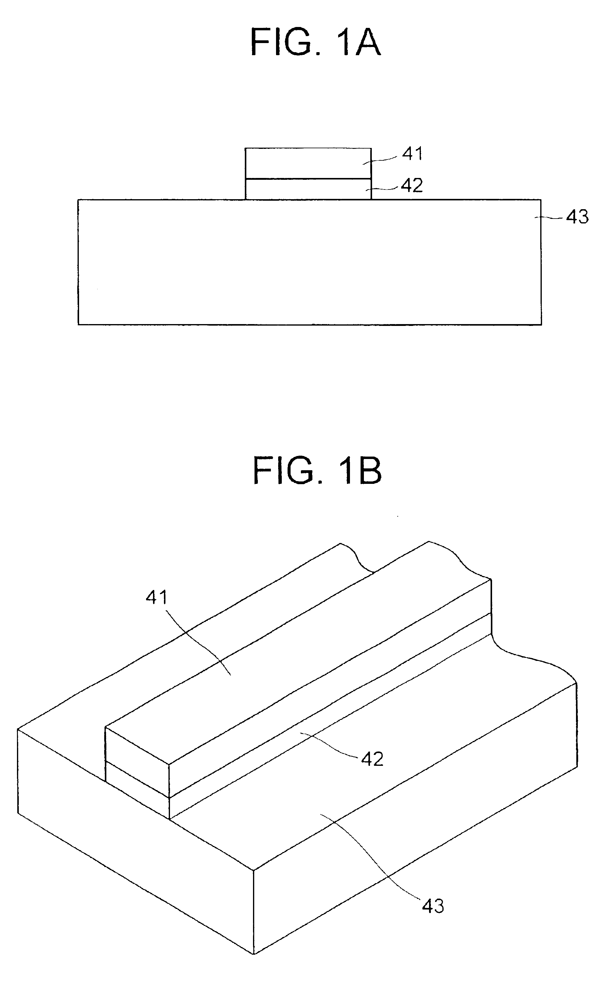
[0071]Referring to FIGS. 1A and 1B, there is shown a structure of a line device according to a first embodiment of the present invention. An interconnect line 41 of the line device is formed on a p-type or n-type semiconductor substrate 43 with an intervention of an insulator film 42. The interconnect line 41 forms a part of a power-source distribution line (referred to as simply distribution line hereinafter) which supplies power to the switching device.

[0072]The semiconductor substrate 43 may be made of any of known semiconductor materials, and may be preferably silicon in view of the feasibility of the fabrication procedure. Examples of the material for the insulator film 42 include SiO2, SiO, SiN, TaO2, TiO2, Al2O3, MgO, SrTiO3, ZrO2 and LaAlO3, but are not limited thereto. Each of these insulators may be used alone or in combination with one or more of other recited insulators. These oxide films have excellent conformity with the silicon semiconductor process, and thus suited a...

second embodiment

[0078]Next, a second embodiment will be described with reference to FIGS. 3A to 3C, wherein an insulator film such as used as a gate oxide film in a general semiconductor circuit is used in the line device to underlie the interconnect line.

[0079]The line device shown in these drawings has a structure similar to a MOSFET, including a portion of a semiconductor (silicon) substrate 43 receiving therein diffused regions 45 and 46, an oxide film 47 formed on the semiconductor substrate 43 between the diffused regions 45 and 46 as viewed from above, and an interconnect line 48 formed on the oxide film 47. The interconnect line 48 forms a part of the distribution line to supply power source voltage.

[0080]The diffused regions 45 and 46 are received in a region encircled by a field oxide film 44, which isolates the region from other regions. The diffused regions 45 and 46 are maintained at the ground potential. The diffused regions 45 and 46 may have a conductivity type same as or opposite t...

third embodiment

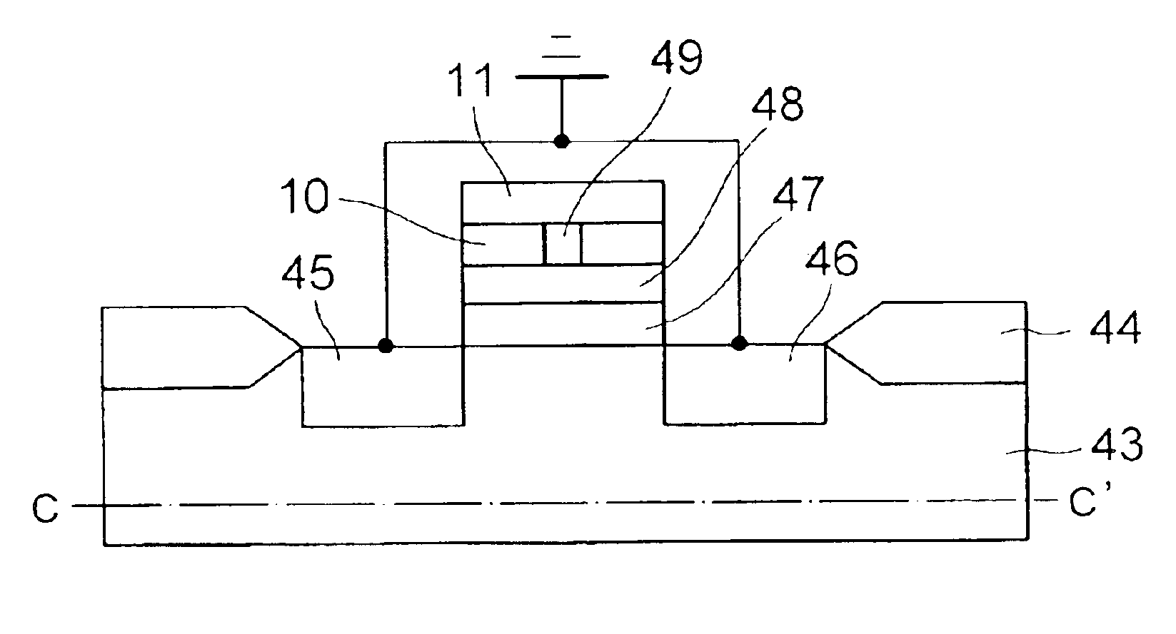
[0091]Referring to FIGS. 6A, 6B and 6C, there is shown a line device according to a third embodiment of the present invention, which is similar to the second embodiment except that the resistance of the interconnect line 48 having a structure of a gate electrode line is reduced by forming a bypass line or associated interconnect line.

[0092]More specifically, the interconnect line 48 is associated with a metallic interconnect line 11 formed on an interlevel dielectric film 10 overlying the interconnect line 48. The associated interconnect line 11 has a width similar to the width of the interconnect line 48 and extends parallel thereto. The associated interconnect line 11 is connected to the interconnect line 48 via contact plugs 49 penetrating the interlevel dielectric film 10 and arranged along the interconnect line 48. In this embodiment, the interconnect line 48, contact plugs 49 and the associated interconnect line 11 form a part of the distribution line, which supplies power sou...


PUM


Abstract

A decoupling device for decoupling a high-frequency noise wave in a digital circuit is formed as a line device including a portion of a semiconductor substrate, an insulator film formed thereon as a gate oxide film, and an interconnect line formed thereon as a gate electrode. The line capacitance between the interconnect line and the semiconductor substrate is 100 pF or above, whereby the decoupling device effectively decouples the electromagnetic noise wave generated by a switching device in a frequency range between 10 and 1000 GHz.

Description

BACKGROUND OF THE INVENTION[0001](a) Field of the Invention[0002]The present invention relates to a low-impedance decoupling device and, more particularly, to a low-impedance decoupling device implemented as a line device and suitably used for decoupling an electromagnetic noise wave in a high-frequency LSI.[0003](b) Description of the Related Art[0004]Electromagnetic interference is caused by an electromagnetic wave induced by a switching operation of a semiconductor element used as a switching device in a digital circuit. The electromagnetic wave includes high-harmonic wave components of a clock frequency, or fundamental wave, which cause high-frequency noise in the semiconductor circuit. Some of the high-frequency electromagnetic wave components generated by the switching device in the LSI are coupled with the signal lines etc. in the LSI, package or printed circuit board (PCB) by induction coupling while the electromagnetic components transfer along a power-source distribution l...

Claims


Application Information

Patent Timeline
Patent Type & Authority Patents(United States)
IPC IPC(8): H01L23/52H01L23/522H01L23/58H01L23/64H01L21/822H01L21/3205H01L27/04
CPCH01L23/5222H01L23/642H01L2924/0002H01L2924/3011H01L2924/00H01L27/04
Inventor NAKANO, TAKASHITOHYA, HIROKAZU
Owner LENOVO INNOVATIONS LTD HONG KONG
Learn More