

Optical pulse code recognition device and optical distributor
a recognition device and optical distributor technology, applied in the direction of instruments, cladded optical fibres, optical elements, etc., can solve the problems of higher bit-rate signals of 100 gbps or 1 tbps not being processed, the recognition circuit design is more complex, and the current upper limit of electronic processing speed is 10 gbps or 40 gbps
- Summary
- Abstract
- Description
- Claims
- Application Information
AI Technical Summary
Benefits of technology
Problems solved by technology
Method used
Image

Examples
first embodiment
(First Embodiment)
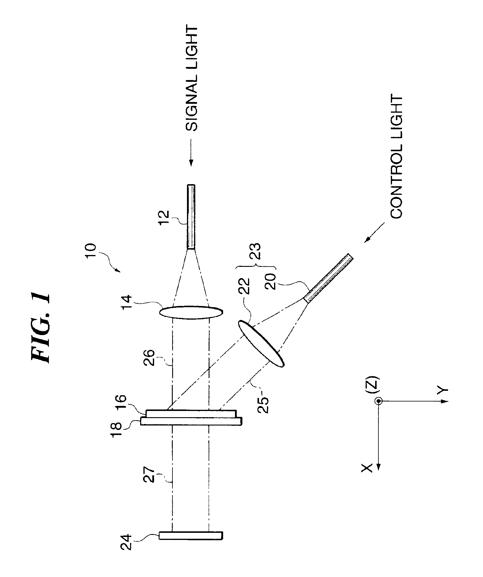
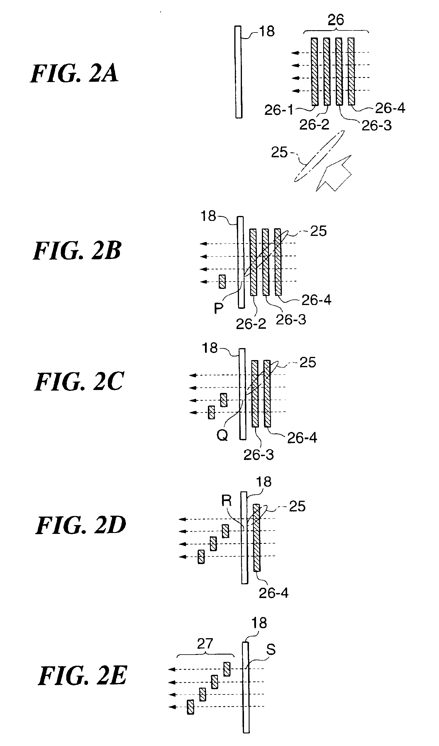
[0053]FIG. 1 is a schematic diagram showing the optical pulse code recognition device 10 of the present invention. As FIG. 1 shows, the optical pulse code recognition device 10 is provided with an optical fiber 12 for emitting a signal light, a lens 14 to collimate a serial signal light of a pulse train emitted from the optical fiber 12, a mask 16 formed in a mask pattern to transmit a portion of the signal light collimated by the lens 14 according to a predetermined pattern, a thin-film optical switch 18 acting as a spatial optical switch that changes the optical transmittance when a control light pulse is applied thereto, a control light emitter 23 containing an optical fiber 20 and a lens 22 to emit a light from a control light generator (not shown in drawing) and a photodetector 24 to detect the signal light transmitted through the thin-film optical switch 18.
[0054]The lens 14 transforms a packet code (serial signal) including a terabit-order light signal pulse...
second embodiment
(Second Embodiment)
[0104]The second embodiment of the present invention is described next. A different mask pattern is described in the second embodiment. Components identical to the embodiments described previously are assigned with same numbers and their detailed description is omitted.
[0105]This embodiment describes the case of expressing N (=2mCm) pieces of information with 2m transmission bits. Mask patterns of 2m bits having m pieces of “1” bits and m pieces of “0” bits are utilized. Examples of bit patterns are shown below in Table 3.
[0106]
TABLE 32 mBit pattern2011040011010101101001101011006000111001011010011100011100101101001110001110010110100111000001101011001001110011100101100100110010101101010010110011010......
[0107]The number of bit pattern combinations is expressed by N=2mCm. For example, when 2m=6(m=3), then N=6C3=20, and 20 bit patterns are present. To recognize all of these patterns, 20 mask patterns are required. Therefore, N types of mask patterns are formed on the...
third embodiment
(Third Embodiment)
[0119]The third embodiment of the present invention is described next. A different configuration of the optical pulse signal recognition device is described in the third embodiment. Components identical to the previous embodiments are assigned with same numbers and their detailed description is omitted.
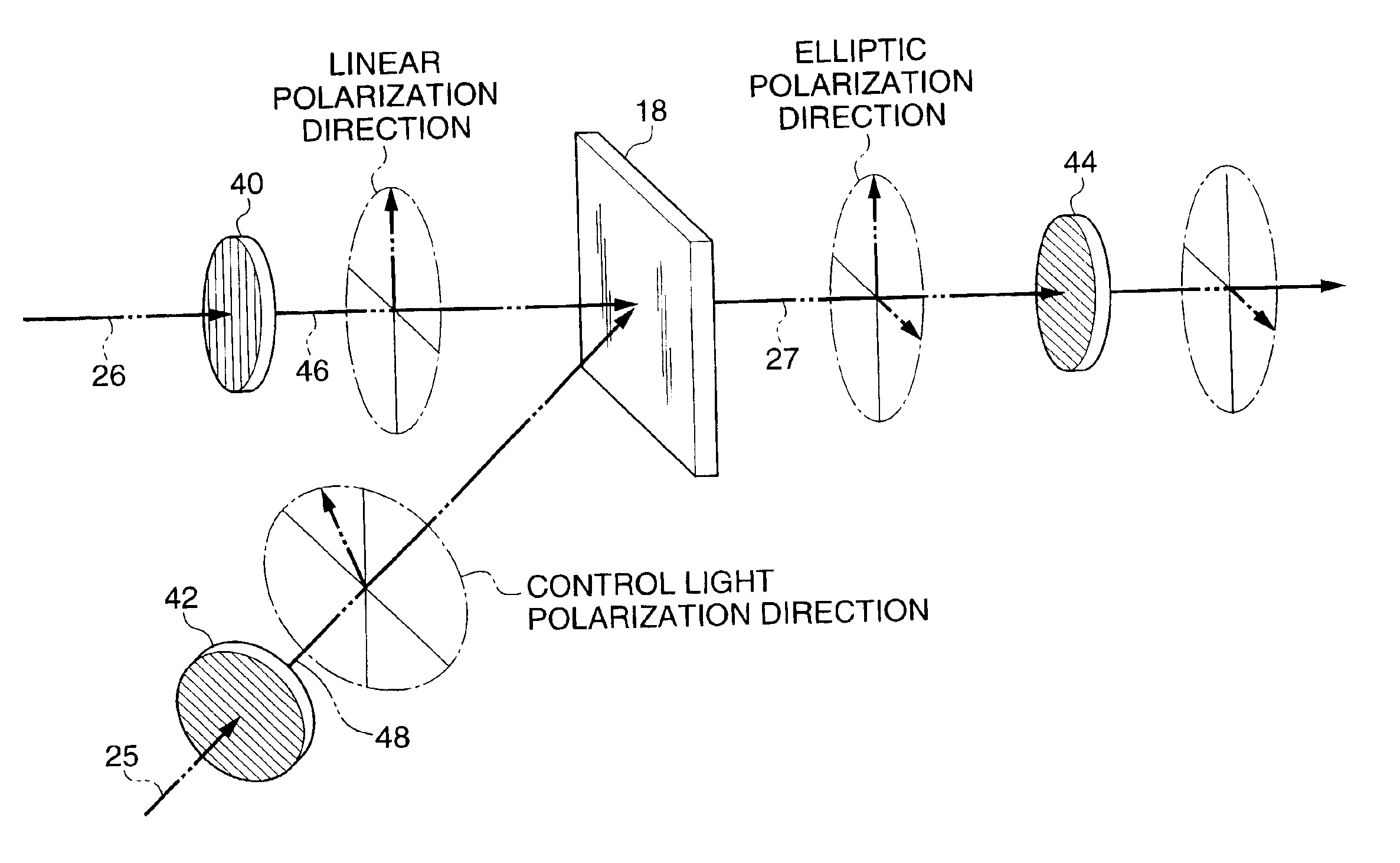
[0120]FIG. 10 is a schematic diagram showing the basic structure of the optical pulse code recognition device of the present embodiment. As shown in FIG. 10, an optical pulse code recognition device 100 has a polarizer 40 interposed between the lens 14 and the mask 16, along the optical path of the collimated signal light 26. A second polarizer 42 is installed on the optical path of the control light 25, between the lens 22 and the mask 16. Further, an analyzer 44 is interposed between the thin film optical switch 18 and the photodetector 24, along the optical path of the parallel signal light 27. Other components of the structure are identical to the previous embodi...
PUM
 Abstract
Description
Claims
Application Information