Fabrication of nano-scale temperature sensors and heaters

a technology of applied in the field of fabrication of nano-scale temperature sensors and heaters, can solve the problems of inconvenient high temperature use of semiconductor diodes, inability to meet high temperature, and large size of sensors, and achieve the effect of high sensitivity

Inactive Publication Date: 2005-06-14
CENT FLORIDA UNIV OF
View PDF12 Cites 21 Cited by
  • Summary
  • Abstract
  • Description
  • Claims
  • Application Information

AI Technical Summary

Benefits of technology

[0006]The second objective of this invention is to provide a method of producing a temperature sensor with a very high sensitivity.

Problems solved by technology

For example, the thermocouple is extremely simple in design and inexpensive, while the semiconductor diode is not suitable for high temperature but used extensively to measure cryogenic temperature.
But near field thermometry involves complicated optical instrumentation and is very cumbersome.
However, it should be noted that the size of their sensors is still limited by the lithographic technique used.
In addition, thermoelectricity of certain bulk materials drop drastically due to the constricted geometry of the AFM tip arrangement.

Method used


Image

  • Fabrication of nano-scale temperature sensors and heaters
  • Fabrication of nano-scale temperature sensors and heaters
  • Fabrication of nano-scale temperature sensors and heaters

Examples


Embodiment Construction

[0019]Before explaining the disclosed embodiment of the present invention in detail it is to be understood that the invention is not limited in its application to the details of the particular arrangement shown since the invention is capable of other embodiments. Also, the terminology used herein is for the purpose of description and not of limitation.

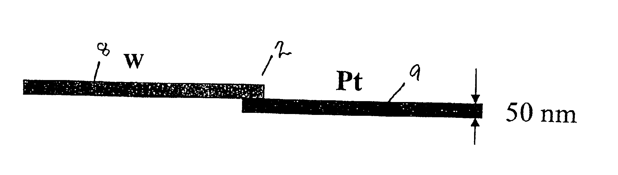
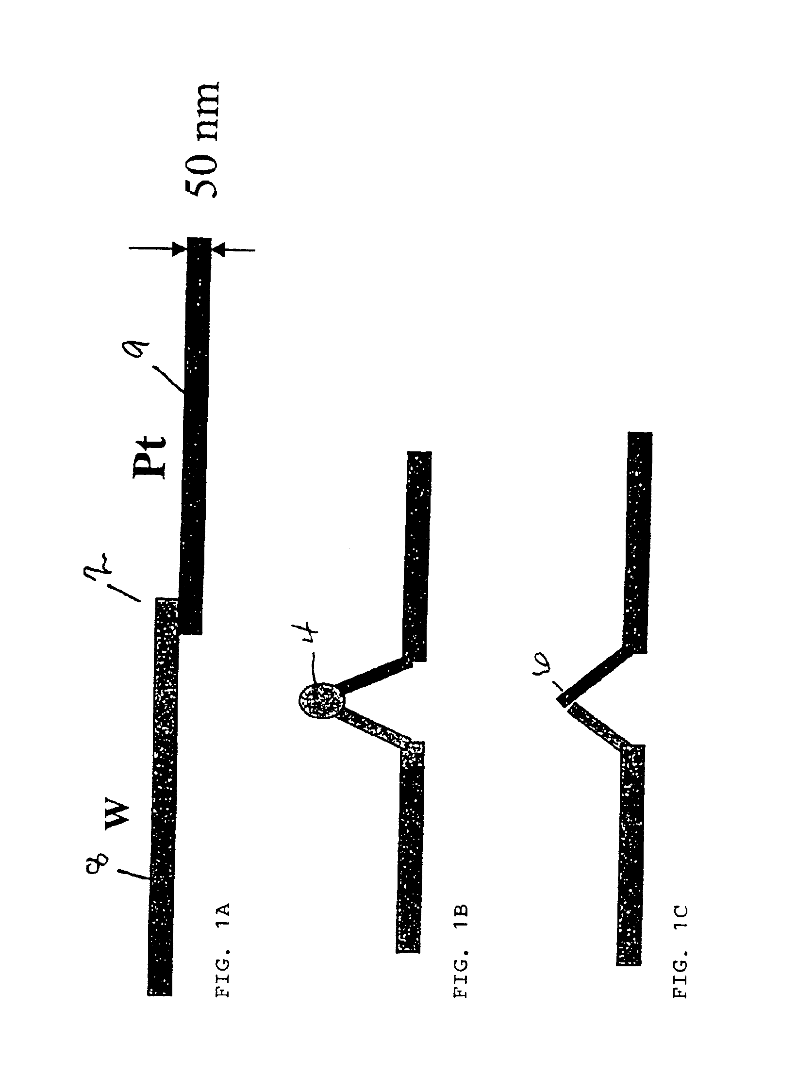
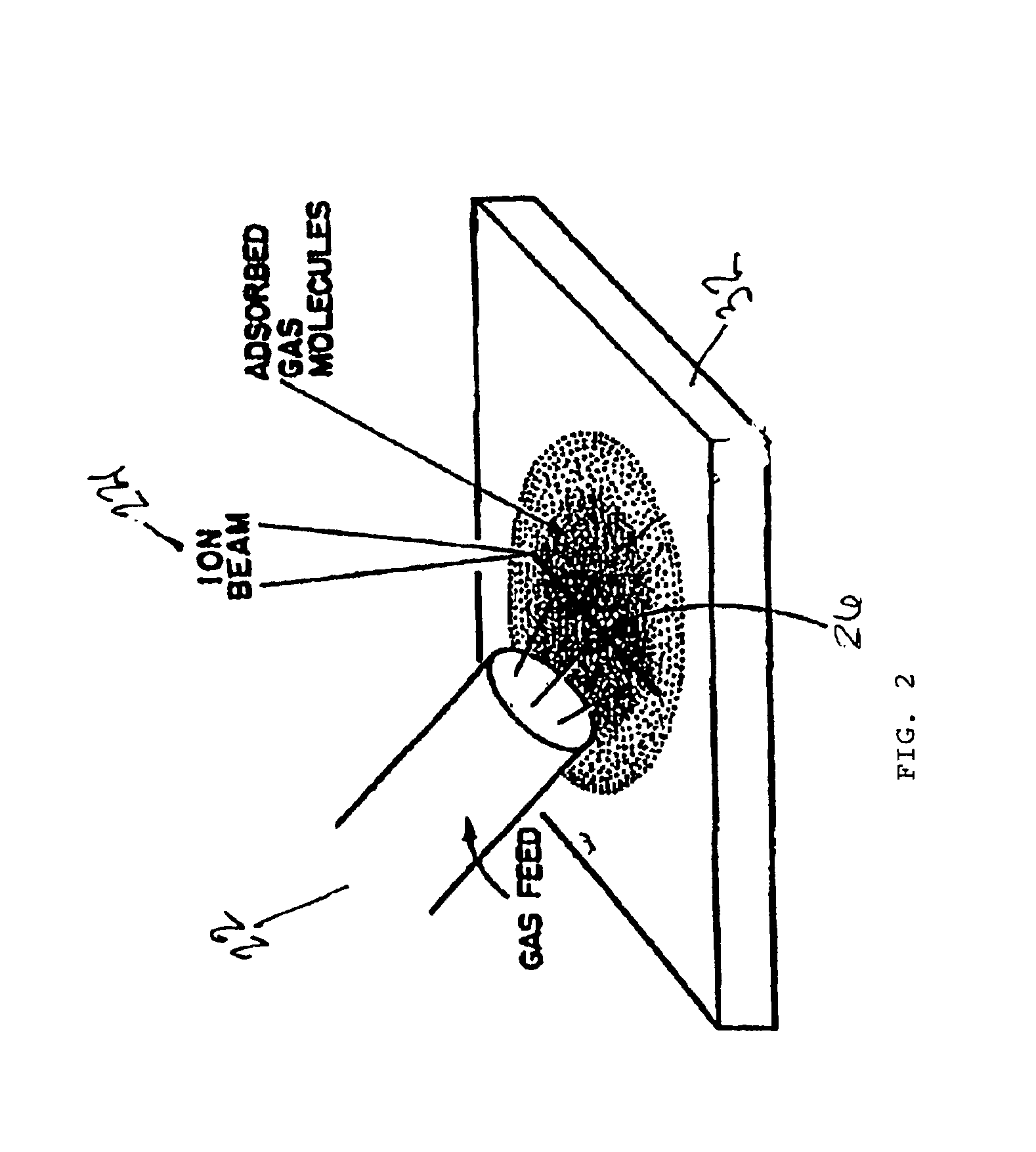
[0020]The method of the invention is based on the discovery that it is possible to create a nano-scale temperature sensor by a FIB (Focused Ion Beam) technique in which the separate nano-strips of W and Pt are deposited onto a substrate through a FIB deposition process. The junction of W and Pt nano-strips formed during the FIB process acts as a nano-scale temperature sensor. The diameters of the W and Pt nano-strips will be on the order of approximately 50 nm, and the cross-sectional area of W / Pt junction will be on the order of approximately 50×50 nm2, which will be the smallest temperature sensors that can be made so far. The ends o...


PUM

PropertyMeasurementUnit
thicknessaaaaaaaaaa
areaaaaaaaaaaa
sizeaaaaaaaaaa

Abstract

The method for the fabrication of nano scale temperature sensors and nano scale heaters using focused ion beam (FIB) techniques. The process used to deposit metal nano strips to form a sensor is ion beam assisted chemical vapor deposition (CVD). The FIB Ga+ ion beam can be used to decompose W(CO)6 molecules to deposit a tungsten nano-strip on a suitable substrate. The same substrate can also be used for Pt nano-strip deposition. The precursors for the Pt can be trimethyl platinum (CH3)3Pt in the present case. Because of the Ga+ beam used in the deposition, both Pt and W nano-strips can contain a certain percentage of Ga impurities, which we denoted as Pt(Ga) and W(Ga) respectively. Our characterization of the response of this Pt(Ga)/W(Ga) nano scale junction indicates it has a temperature coefficient of approximately 5.4 mV/° C. This is a factor of approximately 130 larger than the conventional K-type thermocouples.

Description

[0001]This invention relates to nano scale systems and more particularly relates to nano scale temperature sensors and heaters, their method of fabrication and apparatus for doing so and claims the benefit of priority to U.S. Provisional Application Ser. No. 60 / 272,155 filed on Feb. 28, 2001.BACKGROUND AND PRIOR ART[0002]As semiconductor devices continue to decrease in size and more and more applications have been found for the micro and nano-devices, there is an urgent need for measuring physical quantities at sub-micrometer or even nanometer size dimension. Temperature is one of the findamental physical quantities that routinely needs to be measured in order to derive other thermodynamic quantities such as heat, energy, or specific heat capacity.[0003]Presently temperature can be measured using a thermocouple, a semiconductor diode, a metallic resistor, a thermister, an infrared thermometry, a near-field thermnometry, and other more exotic methods. Each technique has its own advan...

Claims


Application Information

Patent Timeline
Patent Type & Authority Patents(United States)
IPC IPC(8): B05D5/12C23C14/16C23C14/14C23C16/04C23C16/16C23C16/48G01K7/02
CPCC23C16/047C23C16/486G01K7/028C23C16/16B82Y15/00G01K2211/00
Inventor CHOW, LEEZHOU, DANSTEVIE, FRED
Owner CENT FLORIDA UNIV OF
Why Eureka
Try Eureka