Semiconductor device assemblies and packages including multiple semiconductor devices and methods

a technology of semiconductor devices and semiconductor devices, applied in the direction of printed circuit manufacturing, printed circuit electric connection formation, printed circuit aspects, etc., can solve the problems of large footprint devices, large footprint devices, and inconvenient placement of semiconductor devices, so as to reduce the interposer area required for connections, reduce the thickness of the package, and facilitate the positioning of one or more semiconductor devices.

Inactive Publication Date: 2005-06-14
MICRON TECH INC
View PDF17 Cites 208 Cited by
  • Summary
  • Abstract
  • Description
  • Claims
  • Application Information

AI Technical Summary

Benefits of technology

[0016]A “second-level” (e.g., upper) semiconductor device is at least partially superimposed relative to the interposer and generally to the first-level semiconductor device(s) within the interposer receptacle. The second-level semiconductor device may have its active surface facing upwardly, with its bond pads electrically connected to corresponding contact areas on the upper surface of the interposer by way of somewhat laterally extending intermediate conductive elements. Alternatively, peripheral contact areas on the second-level semiconductor device may be flip-chip bonded to contact areas on the interposer. If the first-level semiconductor device is flip-chip connected to corresponding contact areas on the active surface of the second-level semiconductor device, the active surfaces of the first- and second-level semiconductor devices face each other. Conductive traces and vias extend from the conductive areas on the interposer to corresponding out

Problems solved by technology

As with the flat packages, conventional flip-chip type packages are often undesirably thick for use in small, thin, state of the art electronic devices.
Furthermore, use of this general construction method for producing a stacked multichip module (MCM) results in a relatively high-profile, large footprint device.
While interposers that include recesses for partially receiving semiconductor devices facilitate the fabrication of thinner flip-chip type packages, the semiconductor dice of these packages, as well as intermediate conductive elements that protrude beyond the outer surfaces of either the semiconductor dice or the inter

Method used


Image

  • Semiconductor device assemblies and packages including multiple semiconductor devices and methods
  • Semiconductor device assemblies and packages including multiple semiconductor devices and methods
  • Semiconductor device assemblies and packages including multiple semiconductor devices and methods

Examples


Embodiment Construction

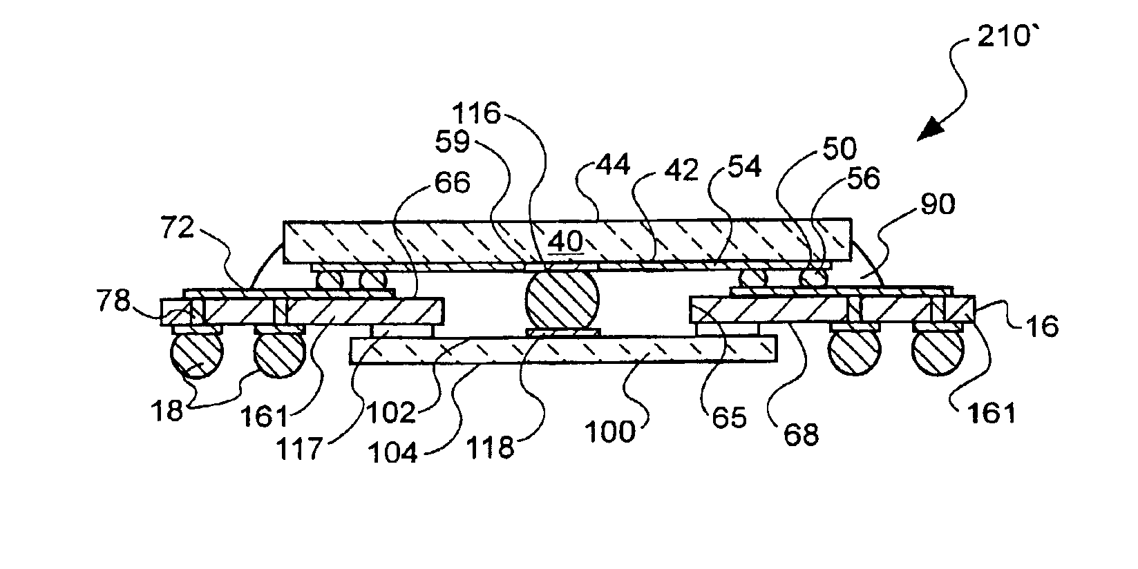
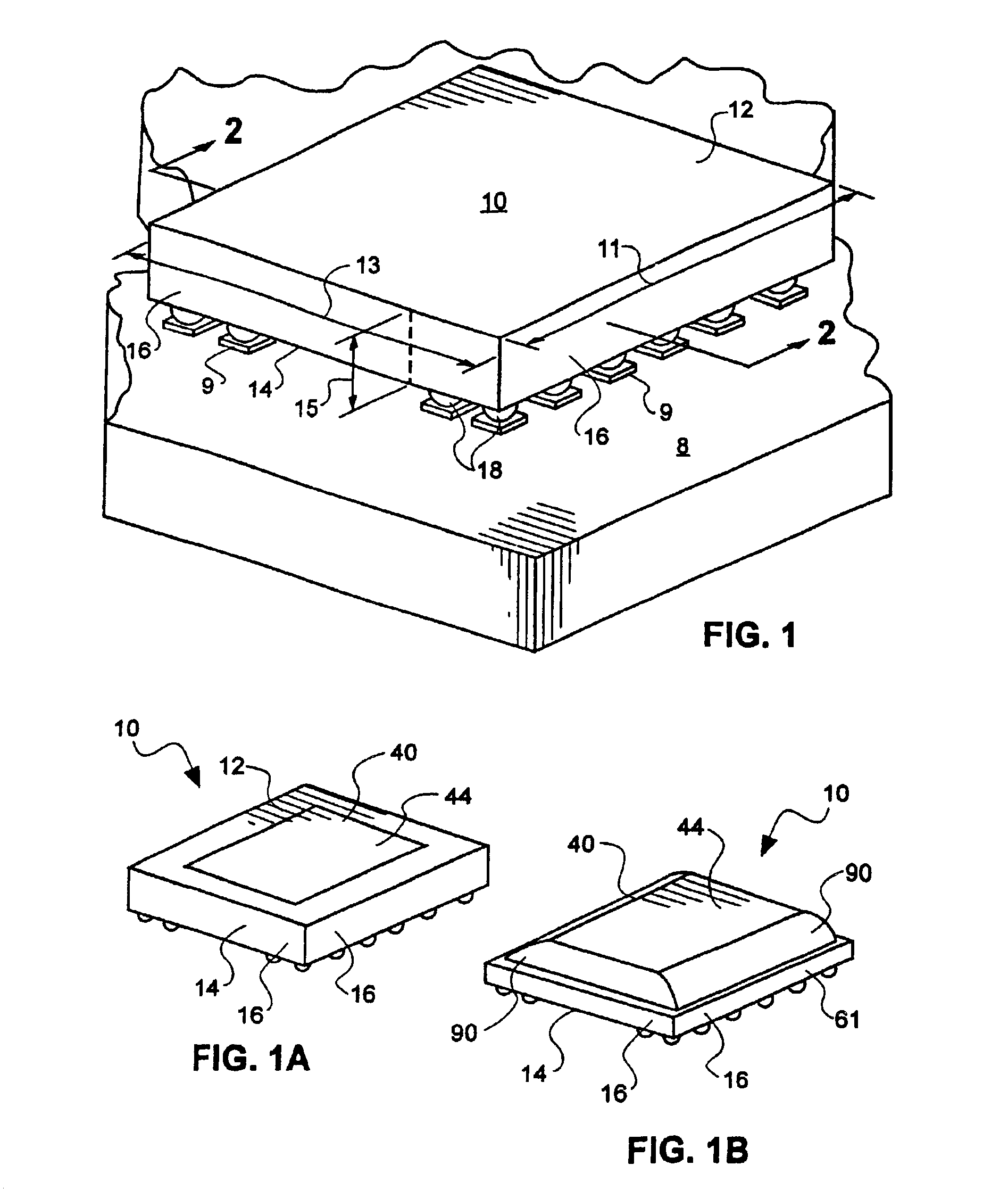
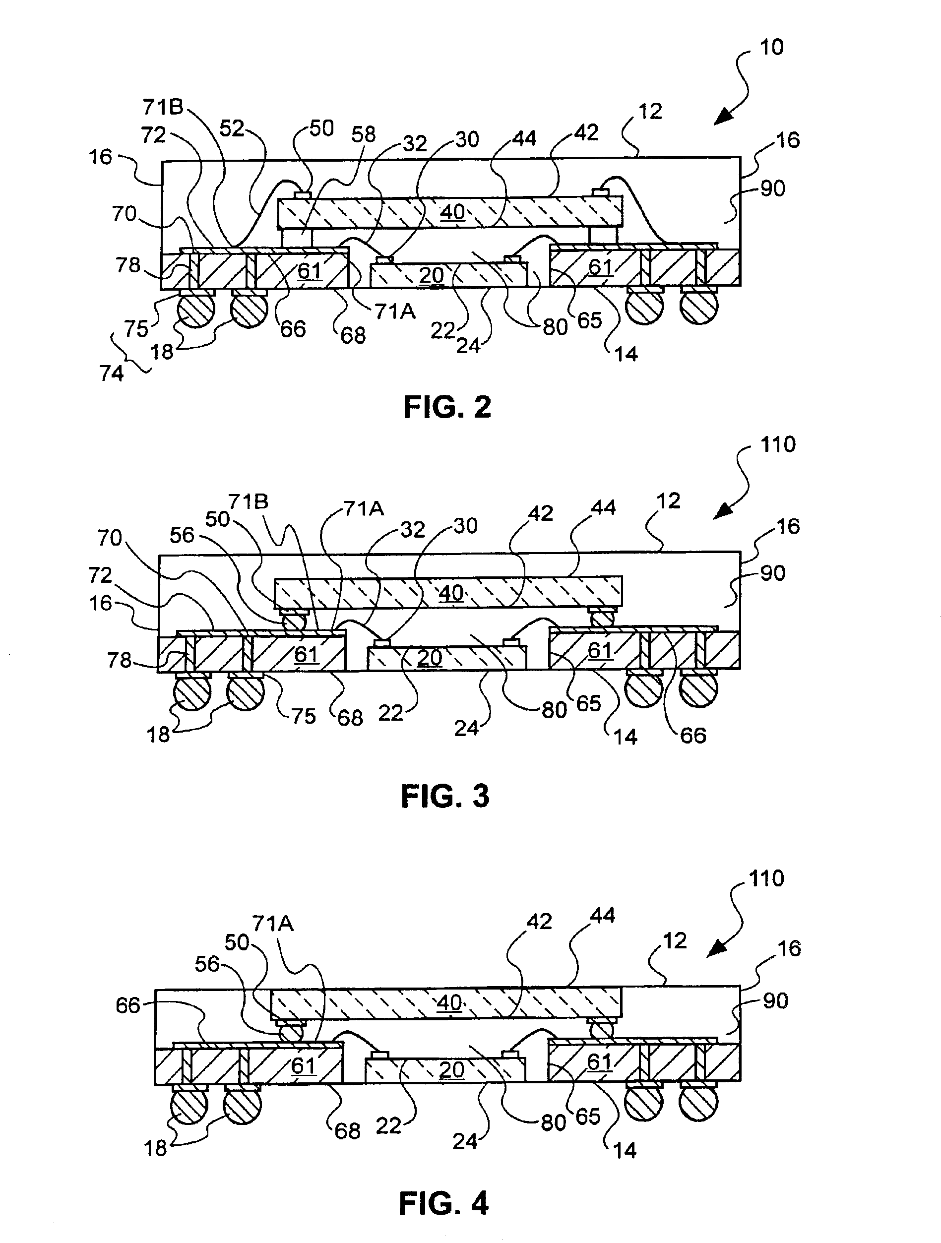
[0053]Referring to FIG. 1, a multichip semiconductor device package 10 according to the present invention is illustrated. As shown, FIG. 1 is an external view of the package 10 and is representative of a large number of possible device configurations exemplified in the figures following FIG. 1. Package 10 is illustrated as having an upper surface 12, a lower surface 14, and peripheral edges 16. Outer connectors 18, shown here as solder balls in a ball grid array (BGA) connection pattern, are depicted as being on the lower surface 14 of the package 10 and attached to contact areas 9 on a representative carrier substrate 8. The dimensions of the package 10 include length 11, width 13 and thickness 15 (exclusive of the distance outer connectors 18 protrude from the lower surface 14). The outline of the encapsulated package 10, comprising length 11 and width 13 dimensions, defines the “footprint” of the package 10. The package 10 shown in FIG. 1 represents a multidie package which has b...


PUM


Abstract

A multidie semiconductor device (MDSCD) package includes a generally planar interposer comprising a substrate with a central receptacle, upper surface conductors, and outer connectors on the lower surface of the interposer. Conductive vias connect upper surface conductors with outer connectors. One or more semiconductor devices may be mounted in the receptacle and one or more other semiconductor devices mounted above and/or below the interposer and attached thereto. The package may be configured to have a footprint not significantly larger than the footprint of the largest device and/or a thickness not significantly greater than the combined thickness of included devices. Methods for assembling and encapsulating packages from multidie wafers and multi-interposer sheets or strips are disclosed. Methods for combining a plurality of packages into a single stacked package are disclosed. The methods may include use of somewhat laterally extending intermediate conductive elements, flip-chip style electrical connection, or both within the same package.

Description

TECHNICAL FIELD[0001]The present invention relates generally to stacked semiconductor device assemblies and packages, as well as to associated assembly and packaging methods. More particularly, the invention pertains to multidie assemblies and packages with low profiles and minimal size.BACKGROUND OF THE INVENTION[0002]The dimensions of many different types of state of the art electronic devices are ever decreasing. To reduce the dimensions of electronic devices, the structures by which the microprocessors, memory devices, other semiconductor devices, and other electronic components of these devices are packaged and assembled with carriers, such as circuit boards, must become more compact. In general, the goal is to economically produce a chip-scale package (CSP) of the smallest size possible, and with conductive structures, such as leads, pins, or conductive bumps, which do not significantly contribute to the overall size in the X, Y, or Z dimensions, all while maintaining a very h...

Claims


Application Information

Patent Timeline
IPC IPC(8): H01L23/28H01L23/31H01L23/498H01L23/48H01L25/10H05K1/14H05K3/40H05K3/34H01L23/13H01L25/065
CPCH01L23/13H01L23/49805H01L25/105H05K1/141H01L23/3128H01L2225/1064H01L2224/16145H01L2924/01078H01L2924/01079H01L2924/09701H01L2924/15311H01L2924/19041H05K3/3436H05K3/3442H05K3/403H05K2201/045H05K2201/049H05K2201/09181H05K2201/10727H01L2924/01087H01L2225/1035H01L24/45H01L24/48H01L24/73H01L24/97H01L25/0657H01L2224/05599H01L2224/16225H01L2224/48091H01L2224/48227H01L2224/73253H01L2224/73265H01L2224/85424H01L2224/85439H01L2224/85444H01L2224/97H01L2225/0651H01L2225/06517H01L2225/0652H01L2225/06555H01L2225/06572H01L2225/06586H01L2225/1023H01L2225/1058H01L2924/00014H01L2924/01005H01L2924/01006H01L2924/01013H01L2924/01033H01L2924/01039H01L2924/01047H01L2924/01049H01L2924/12042H01L2924/15151H01L2924/15331H01L2924/181H01L2924/18161H01L2924/18165H01L2224/32225H01L2924/00012H01L2924/00H01L2224/85H01L2224/81H01L2224/45015H01L2924/207H01L2224/45099
Inventor JIANG, TONGBIFEE, SETHO SINGYEAN, TAY WUUCHYE, LIM THIAM
Owner MICRON TECH INC
Why Eureka
Try Eureka