Non-volatile semiconductor memory device

a non-volatile semiconductor and memory technology, applied in the field of electric eraser programmable read only memory (eeprom) devices, can solve the problems of not being able to detect this kind of fault in any way in program verification schemes, becoming a problem to be solved, and described error bits occurring in program operations

Inactive Publication Date: 2005-06-14
KK TOSHIBA
View PDF5 Cites 203 Cited by
  • Summary
  • Abstract
  • Description
  • Claims
  • Application Information

AI Technical Summary

Problems solved by technology

However, “0” programmed memory cells are accidentally programmed to have an unitentionally high threshold voltage beyond the expected threshold voltage distribution.
Once such an over-program occurs, it becomes impossible to precisely read out a cell data in such a NAND cell unit that includes an over-programmed cell.
Even when the cells that must store logic “1” data improperly behave to store “0” data, prior known program-verify schemes are incapable of detecting this kind of faults in any way.
However, when considering such a copy operation as to copy a certain page data of an EEPROM to another page thereof, above-described error bits occurred in a program operation becomes a problem to be solved, because of that a page data including error bits are programmed to another page as it is.
However, the ECC processing takes time, even if only data check is performed, thereby preventing the speed-up of the page copy operation.
However, even if such the over-program verify operation is added to the program sequence, the reliability of programming is not yet sufficient for achieving a high speed copy operation without use of ECC circuitry.
However, in such the proposed verify method, supposing that a cell threshold of which is nearly equal to 0V is verified as it was normally programmed (“Pass”), it easily becomes erronesously programmed state due to some variation causes after the program sequence.

Method used


Image

  • Non-volatile semiconductor memory device
  • Non-volatile semiconductor memory device
  • Non-volatile semiconductor memory device

Examples


embodiment 1

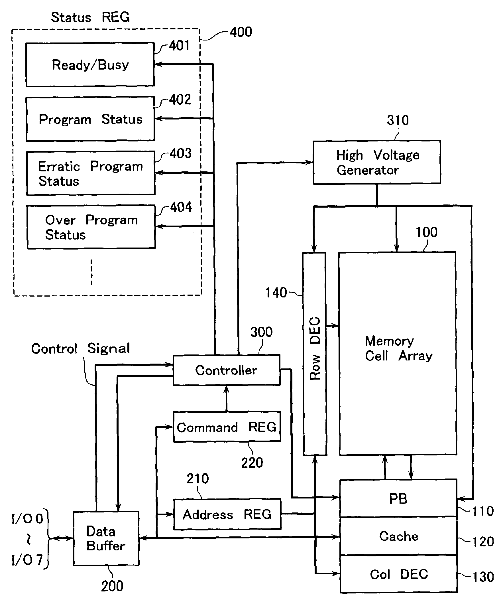
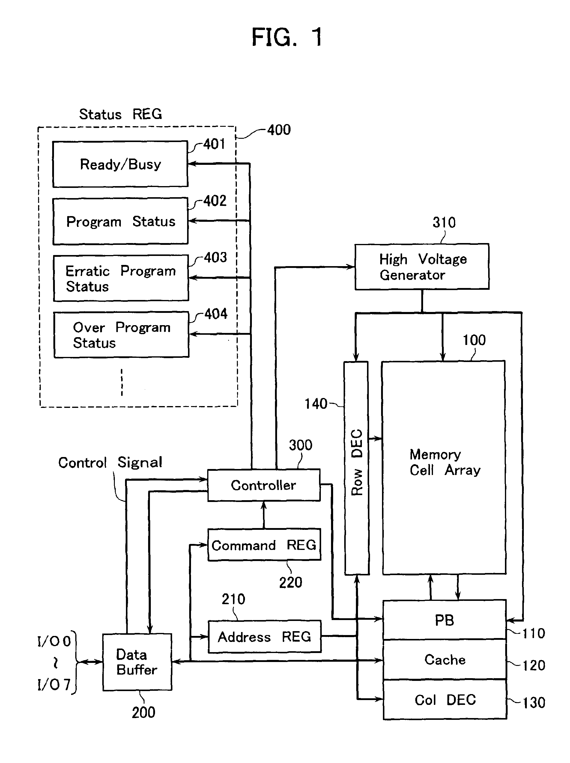
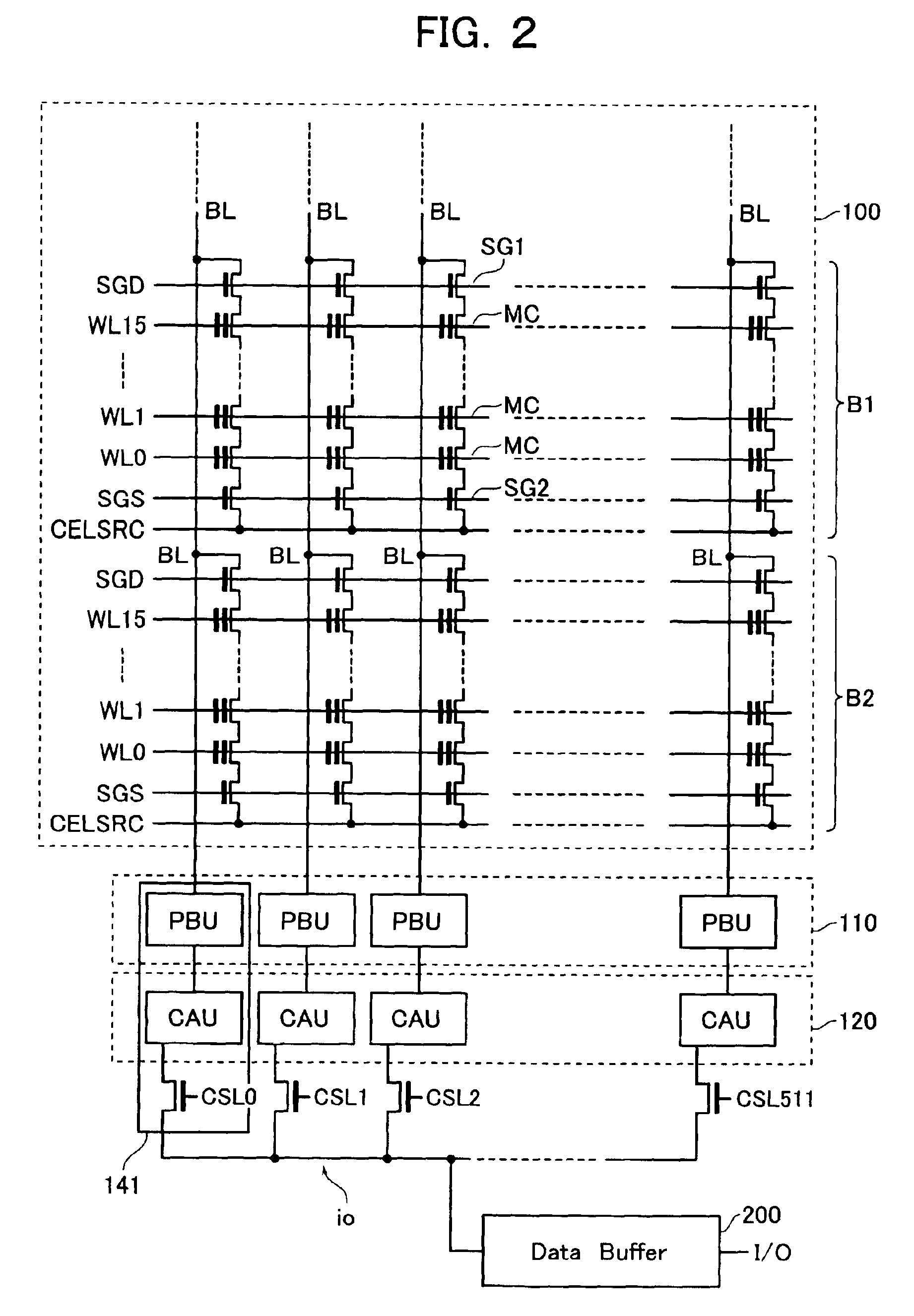
[0041]Referring to FIG. 1, a flash EEPROM memory chip of the NAND type in accordance with an embodiment of this invention is illustrate in block circuit form. The NAND-type flash memory includes array of rows and columns of memory cells indicated by reference numeral 100, a row decoder 140 which performs word-line selection of this memory cell array 100, and a column decoder 130 which performs bit-line selection. Also provided is a page buffer (PB) 110 with a storage capacity corresponding to a page of memory space. The page buffer 110 functions as a sense amplifier circuit which detects or senses data read out of the memory cell array 100, and also acts as a data hold circuit that stores hold program data.

[0042]In currently available NAND flash memory chips, and data bits that have been loaded into the page buffer 110 at the beginning of a program (or write) operation are to be rewritten at the termination of the program operation. In contrast, the illustrative embodiment is specif...

embodiment 2

[0089]An explanation will next be given of another embodiment 2 which is arranged to perform an over-write or over-program verify operation in addition to the erratic program verify operation of the above-noted Embodiment 1. Embodiment 2 is similar in flash memory configuration to Embodiment 1.

[0090]FIG. 7 is a flowchart of an on-chip system routine for operation control, including the over-program verify in this embodiment. This system routine is similar to that of Embodiment 1 in several process steps covering from data load step S1 up to erratic program verify step S7.

[0091]After having performed the erratic program verify operation at step S7, the routine goes to step S8 which checks the data presently held in the page buffer 110 to determine whether an erratic program verify result is “Pass” or not. Recall that “Pass” is set when all data at the node N1 is at “H.” Thus, if Yes at step S8, then the routine proceeds to step S9 which effectuates over program verify. If No at step ...

embodiment 3

[0100]FIG. 18 is a timing diagram of an erratic program verify operation which is little different from that of FIG. 16. In the flow of FIG. 16, the gate voltage BLCLAMP of the clamping NMOS transistor 9 is set at Vpre during bitline precharging and at Vsenev (13.

[0101]When a memory cell needless to be checked during erratic program verify—namely, the node N1 of latch LACTH1 within the page buffer 110—is at “H” (=logic “1” data), the bitline-applied precharge voltage is made equal to Vpre−Vt; during sensing, whether the bitline potential is higher or lower than Vsenev−Vt is the reference for logical judgment. In the pulse signal waveforms during the operation of FIG. 16, the recharge circuit 13 performs recharging of the nodes N4, N1 within the time period between time points EP8 and EP9 in order to avoid unwanted accommodation of the “L” level data to nodes N4, N1 in the case of Vpre−Vt

[0102]In contra...


PUM


Abstract

A non-volatile semiconductor memory device includes a memory cell array, a data hold circuit, and a controller A program control function applies a program voltage to a selected memory cell to let data shift from a first logic state to a second logic state. A program verify control function verifies that a programmed data of the selected memory cell shifted to the second logic state. An erratic program verify control function checks that a threshold voltage of a memory cell to be held in the first logic state does not exceed a third value set as an upper limit value of a variation of the first logic state. An over-program verify control function checks that a threshold voltage of the selected memory cell shifted to the second logic state does not exceed a fourth value set as an upper limit thereof.

Description

CROSS-REFERENCE TO RELATED APPLICATION[0001]This application is based upon and claims the benefit of priority from the prior Japanese Patent Application No. 2001-388347, filed on Dec. 20, 2001, the entire content of which is incorporated herein by reference.BACKGROUND OF THE INVENTION[0002]1. Field of the Invention[0003]This invention relates generally to an electrically erasable programmable read only memory (EEPROM) device. More particularly, the invention relates to programming control techniques adaptable for use with the nonvolatile memory devices.[0004]2. Description of Related Art[0005]EEPROM memory cells are generally designed to employ metal oxide semiconductor (MOS) transistors with stacked structures of a floating gate and a control gate. In flash EEPROM memories of the so-called NAND type, a plurality of memory cells are connected in series together to make up a NAND cell unit. The NAND-type flash memories store data in a nonvolatile way while regarding a threshold volta...

Claims


Application Information

Patent Timeline
Patent Type & Authority Patents(United States)
IPC IPC(8): G11C16/34G11C16/06
CPCG11C16/3454G11C16/3463G11C16/3459
Inventor HOSONO, KOJIIMAMIYA, KENICHINAKAMURA, HIROSHINAKABAYASHI, MIKITOKAWAI, KOICHI
Owner KK TOSHIBA
Why Eureka
Try Eureka