[0007]It is an
advantage of the invention to provide circuits and methods for increasing drive strength and reducing propagation delays of a digital logic circuit.
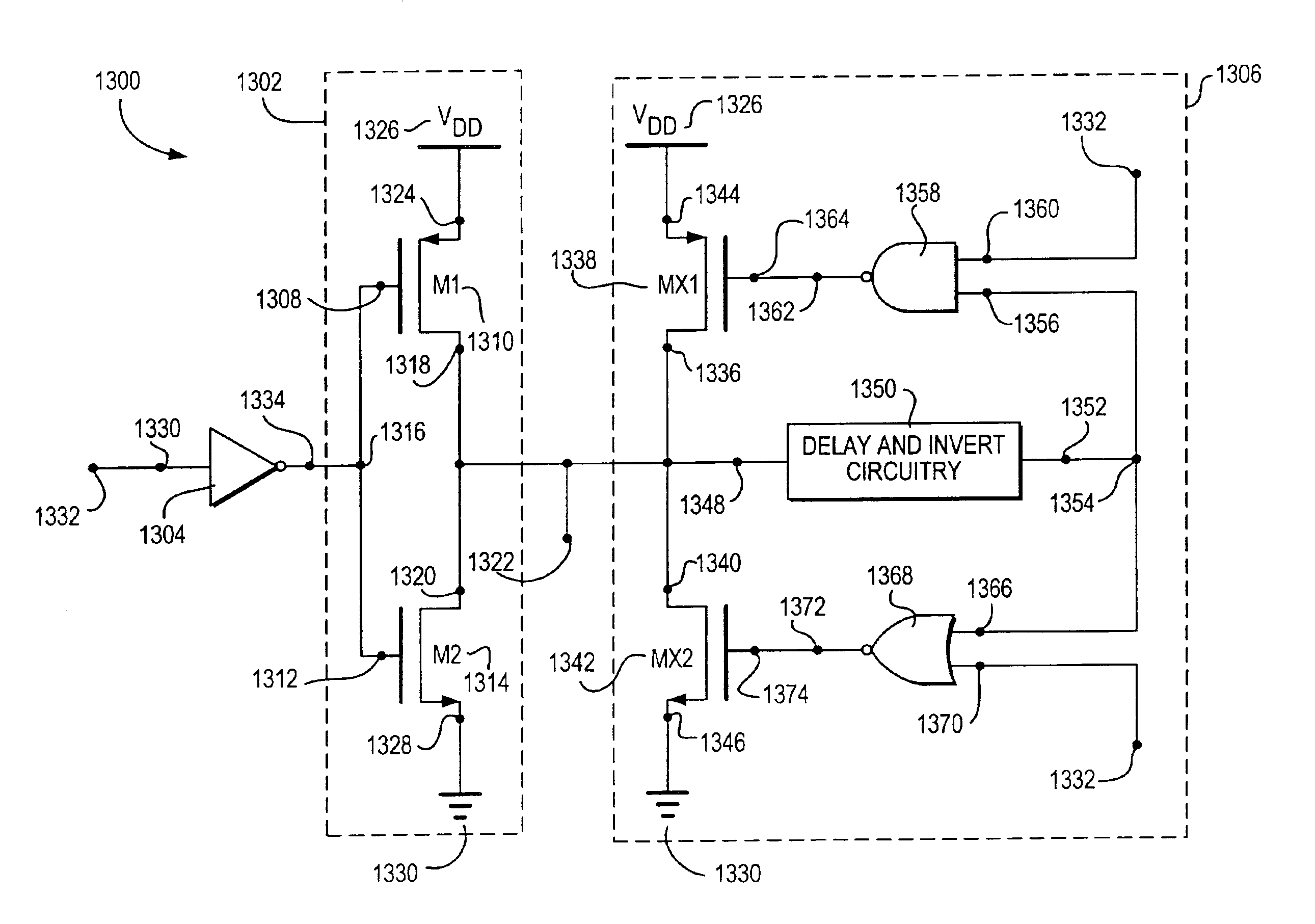
[0008]Circuitry for increasing drive strength of a digital logic circuit through the use of feedback is provided in accordance with the invention.
Logic circuitry turns “ON” a supplemental drive transistor for an output signal digital state transition at an output terminal of the digital logic circuit. The supplemental drive transistor provides supplemental drive current to the digital logic circuit during the output signal digital state transition, thus advantageously reducing
propagation delay and increasing fan-out capability of the digital logic circuit. For example, in one embodiment, a digital logic
NAND gate turns “ON” a first drive transistor for an output signal digital state transition from a digital “0” to a digital “1” at the output terminal of the digital logic circuit, and a digital logic
NOR gate turns “ON” a second drive transistor for an output signal digital state transition from a digital “1” to a digital “0” at the output of the digital logic circuit. A first input terminal of the
logic circuitry is connected to an input terminal of the digital logic circuit. A second input terminal of the
logic circuitry is connected to a delayed version of the output signal from the output terminal of the digital logic circuit. The logic circuitry turns “OFF” an “ON” drive transistor once the output signal digital state transition at the output terminal of the digital logic circuit is complete. In some embodiments, increased drive current is provided during an output
signal transition from a digital “0” to a digital “1” only, or from a digital “1” to a digital “0” only.
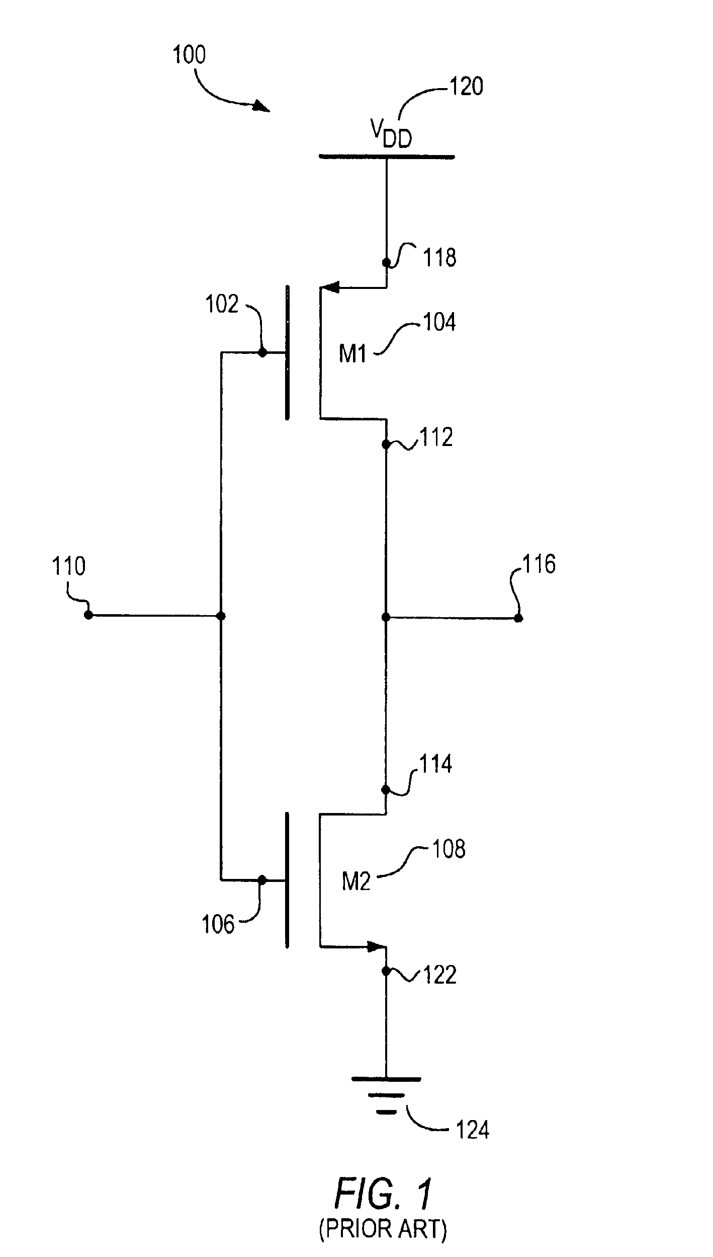
[0009]A modified non-inverting two-stage
CMOS circuit is provided in accordance with the invention. A logic
inverter is connected to the input terminal of a known
CMOS inverter.
Logic circuitry turns “ON” a drive transistor operative to source supplemental drive current during an output signal digital state transition at an output terminal of the
CMOS circuit and turns “OFF” the drive transistor once the output signal digital state transition is complete. For example, in one embodiment, a digital logic
NAND gate turns “ON” a first drive transistor for an output digital state transition from a digital “0” to a digital “1” at the output terminal of the CMOS circuit, and digital logic
NOR gate turns on a second drive transistor for an output digital state transition from a digital “1” to a digital “0” at the output terminal of the modified CMOS circuit. A first input terminal of the logic circuitry is connected to an input terminal of the modified CMOS circuit. A second input terminal of the logic circuitry is connected to a delayed version of the output signal from the output terminal of the modified CMOS circuit. In some embodiments, increased drive current is provided during an output
signal transition from a digital “1” to a digital “0” only, or from a digital “0” to a digital “1” only. The modified non-inverting two-stage CMOS circuit provided in accordance with the invention has advantageously increased drive strength and reduced propagation delays in comparison to a stand-alone known non-inverting two-stage CMOS circuit.
[0010]Methods of increasing drive strength of a digital logic circuit through the use of feedback are provided in accordance with the invention. Responsive to determining that an input signal at an input terminal of the digital logic circuit has transitioned digital states, supplemental drive current is provided to the digital logic circuit during the corresponding output signal digital state transition at an output terminal of the digital logic circuit. In one embodiment, supplemental drive current is provided during an output
signal transition from a digital “1” to a digital “0” at the output terminal of the digital logic circuit. In another embodiment, supplemental drive current is provided during an output signal transition from a digital “0” to a digital “1” at the output terminal of the digital logic circuit. Responsive to determining via a feedback path that the output signal digital state transition is complete, the supplemental drive current is no longer provided to the digital logic circuit. The supplemental drive current advantageously reduces
propagation delay and increases fan-out capability of the digital logic circuit.
[0011]Methods of making a circuit operative to increase drive strength of a digital logic circuit are provided in accordance with the invention.
Delay circuitry operative to receive and
delay an output signal from an output terminal of the digital logic circuit is provided. Also provided is at least one drive transistor operative to source supplemental drive current to the digital logic circuit. Further, logic circuitry is provided. The logic circuitry has a first input terminal connected to an output terminal of the
delay circuitry and a second input terminal connected to an input terminal of the digital logic circuit, and is operative to turn “ON” the drive transistor during an output signal digital state transition at the output terminal of the digital logic circuit and turn “OFF” the drive transistor once the output signal digital state transition is complete.

