

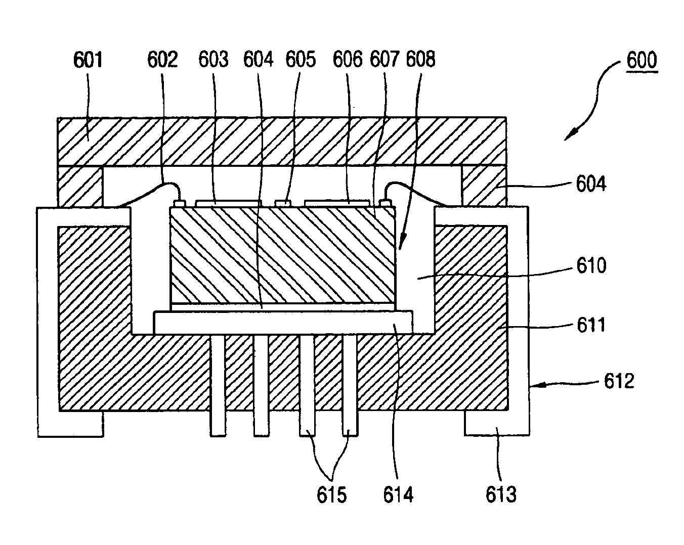
Duplexer filter having film bulk acoustic resonator and semiconductor package thereof
a film bulk acoustic resonator and duplexer technology, which is applied in the direction of generators/motors, fluid pressure measurement, instruments, etc., can solve the problems of large damage risk, large size of general frequency filters using electromagnetic waves, and long time to fabricate film bulk acoustic resonators, etc., to achieve excellent bonding characteristics and excellent characteristic of piezoelectric layers
- Summary
- Abstract
- Description
- Claims
- Application Information
AI Technical Summary
Benefits of technology
Problems solved by technology
Method used
Image

Examples
first embodiment
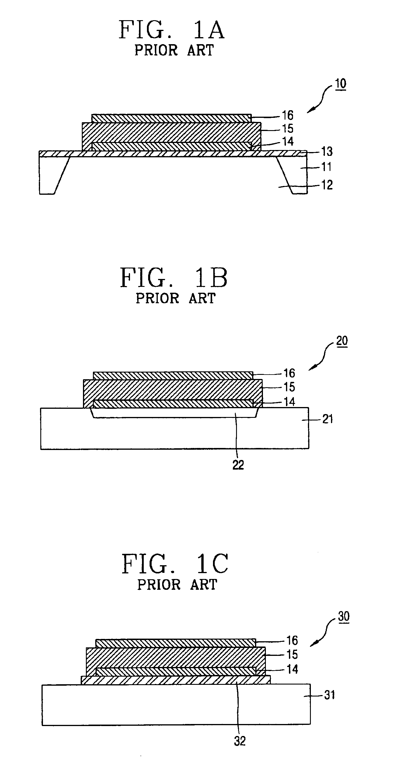
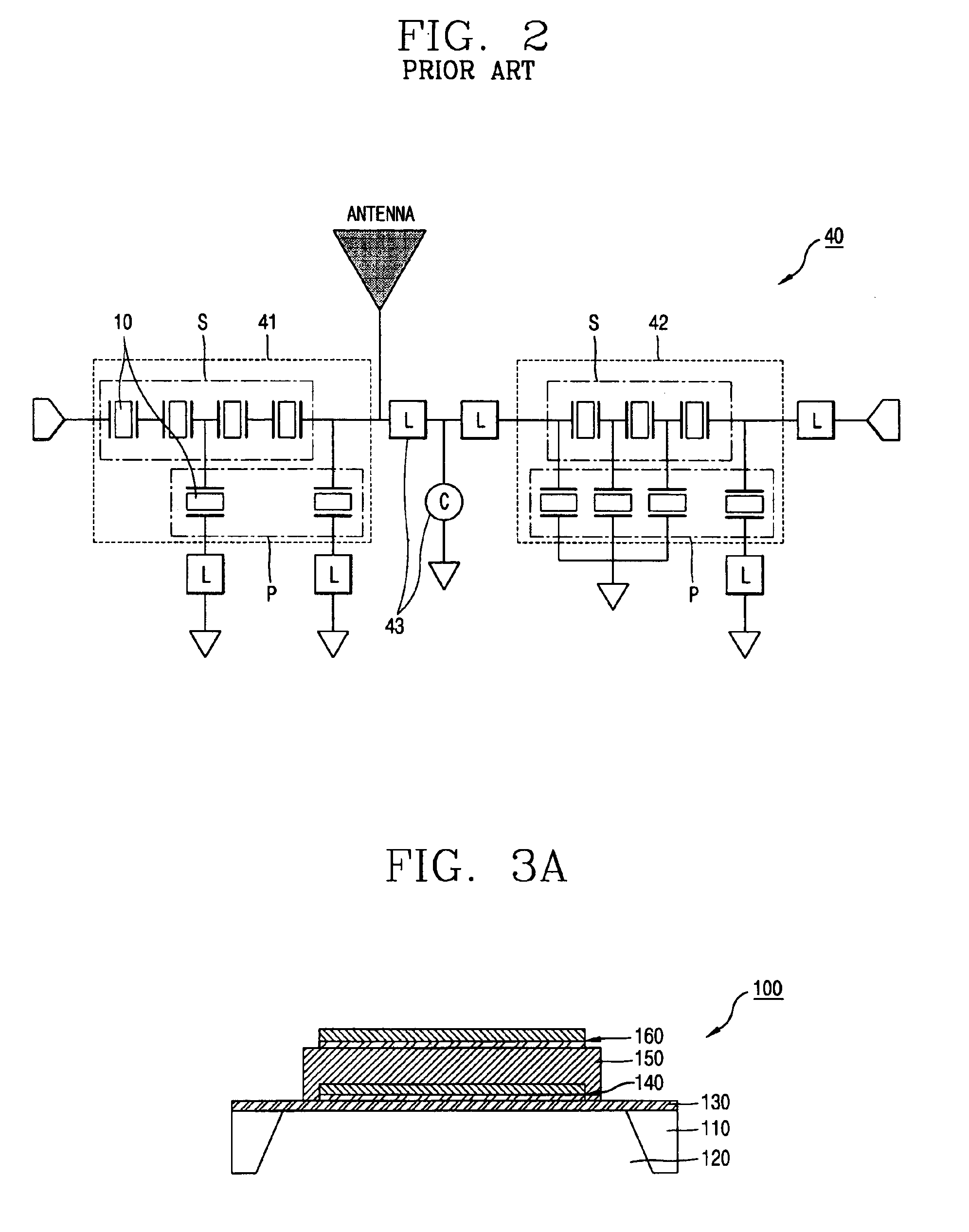
[0053]FIG. 3A is a sectional view showing a film bulk acoustic resonator according to the present invention.
[0054]As shown, the film bulk acoustic resonator 100 according to the first embodiment of the present invention comprises: a semiconductor substrate 110; a film 130 formed on the semiconductor substrate 110; a lower electrode 140 of two layers formed on the film 130; a piezoelectric layer 150 formed on the exposed surface of the lower electrode 140 of two layers; and an upper electrode 160 of two layers formed on the piezoelectric layer 150. The lower electrode 140 of two layers and the upper electrode 160 of two layers can be formed with more than two layers.
[0055]Hereinafter, the construction of the film bulk acoustic resonator according to the first embodiment of the present invention will be explained in more detail.
[0056]The semiconductor substrate 110 can be formed with one of Si, GaAs, or the equivalent material thereof. The semiconductor substrate 110 is not limited to...
second embodiment
[0061]FIG. 3B is a sectional view showing a film bulk acoustic resonator according to the present invention.
[0062]As shown in FIG. 3B, the film bulk acoustic resonator 200 according to the second embodiment of the present invention are similar as the film bulk acoustic resonators 100 shown in FIG. 3A, so that only the differences therebetween will be explained.
[0063]As shown in FIG. 3B, in the film bulk acoustic resonator 200 according to the second embodiment of the present invention, instead of forming the hole 120 at the semiconductor substrate 110, which is a difficult process, an air layer 210 of a predetermined depth is formed at a lower portion of the lower electrode 140. As known, the air layer 210 is formed by etching a sacrificial layer (not shown), and increases the characteristic of the piezoelectric layer 150. The lower electrode 140 and the upper electrode 160 are formed by depositing metal of two layers or more than two layers.
third embodiment
[0064]FIG. 3C is a sectional view showing a film bulk acoustic resonator according to the present invention.
[0065]As shown in FIG. 3C, the film bulk acoustic resonator 300 according to the third embodiment of the present invention is similar as the film bulk acoustic resonator 200 shown in FIG. 3B, so that only the differences therebetween will be explained.
[0066]As shown in FIG. 3C, in the film bulk acoustic resonator 300 according to the third embodiment of the present invention, the hole 120 or the air layer 210 is not formed at the semiconductor substrate 110. That is, an acoustic wave reflective layer 310 of a multi-layer is formed between the lower electrode 140 and the semiconductor substrate 110. The acoustic wave reflective layer 310 can be formed by sequentially depositing SiO2 and W several times, and increases the characteristic of the piezoelectric layer 150. As aforementioned, the lower electrode 140 and the upper electrode 160 are formed by depositing metal of two lay...
PUM
 Abstract
Description
Claims
Application Information