Micro cooling and power supply structure

Active Publication Date: 2005-07-05
IND TECH RES INST
View PDF2 Cites 27 Cited by
  • Summary
  • Abstract
  • Description
  • Claims
  • Application Information

AI Technical Summary

Benefits of technology

[0017]The emitting surface and the collecting surface are parallel to each other and are separated by a vacuum insulation layer having a nanometer range thickness. The plurality of micro cantilever components are formed on the emitting surface by Micro Electro Mechanical System (MEMS) process technology, and the projection parts. sensor components and actuator components are formed by the bulk micromachining and surface micromachining methods of the MEMS process technology. Moreover, the micro cantilever beam components are evenly arranged over the entire emitting surface in an array fashion. And the pre-determined distance maintained between the projection part and the collecting surface is the optimal distance for electrons on the emitting surface to easily produce the electron tunneling effect.
[0018]According to the present invention, the nanometer range electron tunneling gap required is achieved by small adjustments made by the micro cantilever beam componen

Problems solved by technology

But from observing the curves, it can be seen that the heat dissipation efficiency gradually drops if the gap (vacuum insulation layer thickness) between two chips becomes too small.
So, a critical bottleneck for such technology is controlling surface planarity and the position of the two chips, such that their vacuum gap is accurately positioned in the nanometer range and an optimal electron tunneling distance is maintained
However, such a design allows only a fixed gap to be maintained between two chips, but not always the optimal electron tunneling vacuum gap.
And even if the distance changes. by only several nanometers, the cooling and power supply effects can be significantly and often adversely affected (as illustrated in FIG.
It appears unlikely that this method can achieve optimal control of vacuum gap distance over the var

Method used


Image

  • Micro cooling and power supply structure
  • Micro cooling and power supply structure
  • Micro cooling and power supply structure

Examples


Embodiment Construction

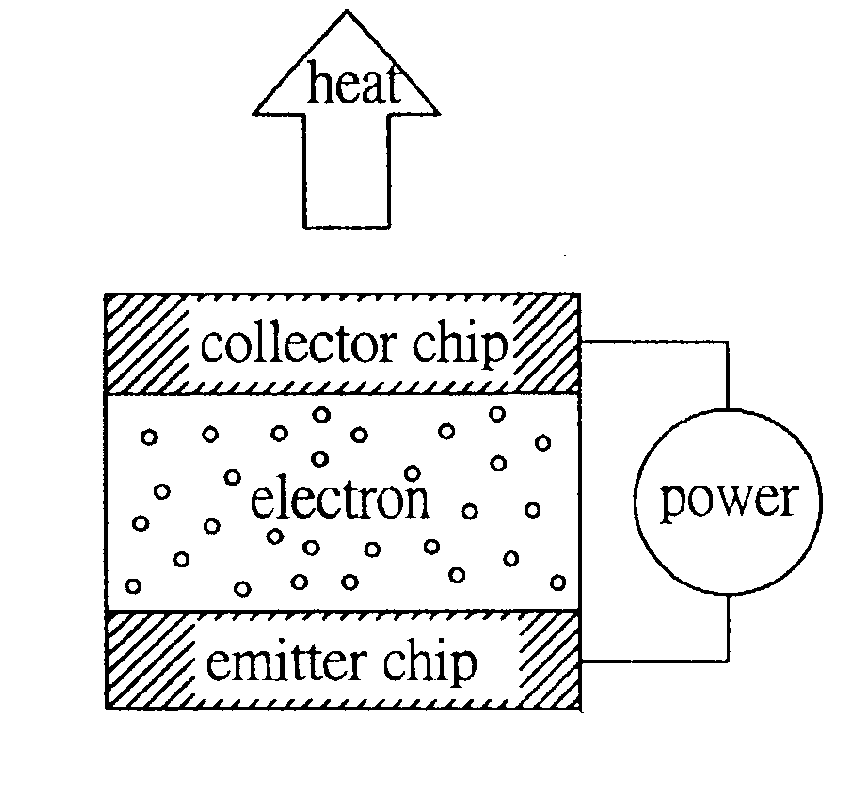
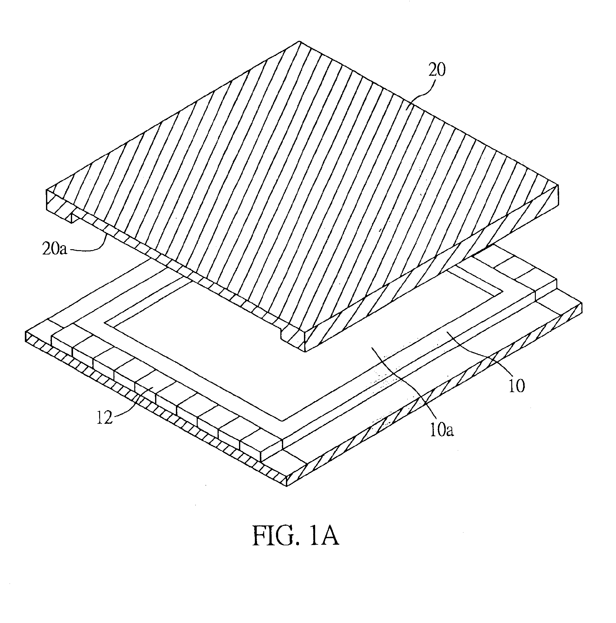
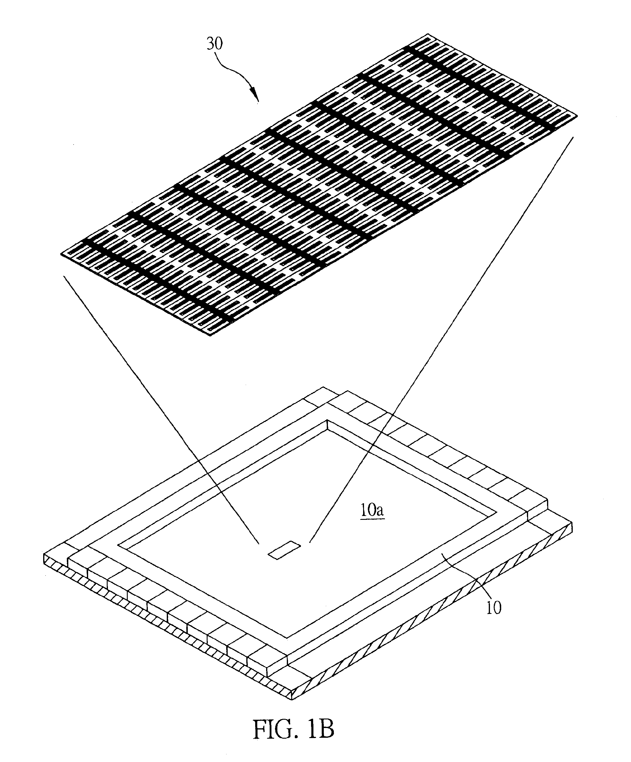
[0031]FIG. 1A, 1B, and 1C are schematic diagrams illustrating a micro cooling and power supply structure according to one preferred embodiment of the present invention. The microstructure is formed with a chip module having an emitter end chip 10 and a collector end chip 20 that is encased above the emitter end chip 10. The emitter end chip 10 has an emitting surface 10a, while the collector end chip 20 has a collecting surface 20a that corresponds to the emitting surface 10a, and the two surfaces 10a, 20a are separated by a vacuum insulation layer having a nanometer range thickness. The emitting surface 10a of the emitter end chip 10 is machined in such a way that it has a micro cantilever beam array structure 30 with from a few thousand to many thousand sets of micro cantilever beam components 31 arranged as shown in FIG. 1B, which enable electrons in the emitter end chip 10 to emit from the micro cantilever beam components 31 and tunnel through the vacuum insulation layer between...


PUM


Abstract

A micro cooling and power supply structure is proposed, which includes an emitter end chip having an emitting surface, a collector end chip having a collecting surface that corresponds to the emitting surface and is separated from the emitting surface, and a plurality of micro cantilever beam components formed on the emitting surface. Each micro cantilever beam component has a projecting part as an electron emitter. A distance between the projecting part and the collecting surface is sensed by a sensor component and maintained by an actuating component at an optimal value to produce an electron tunneling effect, so as to lessen the requirement for a planar chip surface and the low work function material. With the capacity of the micro cantilever beam components to position the tunneling distance, the frequency of electron tunneling to the collecting surface is increased, and excellent cooling and power supply efficiency are achieved.

Description

[0001]This nonprovisional application claims priority under 35 U.S.C. §119 (a) on Patent Application No(s). 092204350 filed in TAIWAN, R.O.C. on Mar. 20, 2003, which is (are) herein incorporated by reference.FIELD OF THE INVENTION[0002]The present invention relates to electron tunneling type micro cooling and power supply structures, and more particularly, to an electron tunneling type micro cooling and power supply structure so as to minimize requirements for chip surface planarity and low work function material.BACKGROUND OF THE INVENTION[0003]The micro cooling and power supply structure refers to a structure in which an electron tunneling effect is produced to shift energy to a collector end chip in a chip module comprising an emitter end chip and the collector end chip which is separated from the emitter end chip by an insulation layer. The electron tunneling effect occurs when the emitter electron absorbs energy to break free from its lattice chain, thereby transmitting energy....

Claims


Application Information

Patent Timeline
IPC IPC(8): B81B3/00H01L23/34H02N10/00F25B21/00H02N1/00H02N11/00
CPCF25B21/00H02N1/006H02N11/006F25B2321/003Y02B30/66Y02B30/00
Inventor LEE, E-IJENG, JING-LYANGYAO, DA-JENGHUANG, I-TE
Owner IND TECH RES INST
Why Eureka
Try Eureka