Method and apparatus for performing rule-based gate shrink utilizing dipole illumination

a dipole illumination and gate shrinking technology, applied in the field of photolithography, can solve the problems of reducing reducing cd (critical dimension) of the corresponding mask pattern approaching the resolution limit of the optical exposure tool, so as to reduce the length of the transistor gate, reduce the length, and reduce the size of the integrated circuit.

Active Publication Date: 2005-07-05
ASML NETHERLANDS BV
View PDF10 Cites 35 Cited by
  • Summary
  • Abstract
  • Description
  • Claims
  • Application Information

AI Technical Summary

Benefits of technology

[0012]In an effort to solve the foregoing needs, it is one object of the present invention to provide a method for reducing the gate length of transistors contained in integrated circuits utilizing currently available photolithography technology. In other words, it is an object of the present invention to provide a method for printing gates exhibiting a reduced length, while maintaining a high level of resolution. Moreover, it is an object of the present invention to allow for the reduction of gate length without requiring a complete resealing of the semiconductor design.

Problems solved by technology

These rules are set by processing and design limitations.
As the size of an integrated circuit is reduced and its density increases, however, the CD (critical dimension) of its corresponding mask pattern approaches the resolution limit of the optical exposure tool.
One issue of particular importance to integrated circuit designers is the ability to reduce the length of the transistor gate as much as possible.

Method used


Image

  • Method and apparatus for performing rule-based gate shrink utilizing dipole illumination
  • Method and apparatus for performing rule-based gate shrink utilizing dipole illumination
  • Method and apparatus for performing rule-based gate shrink utilizing dipole illumination

Examples


Embodiment Construction

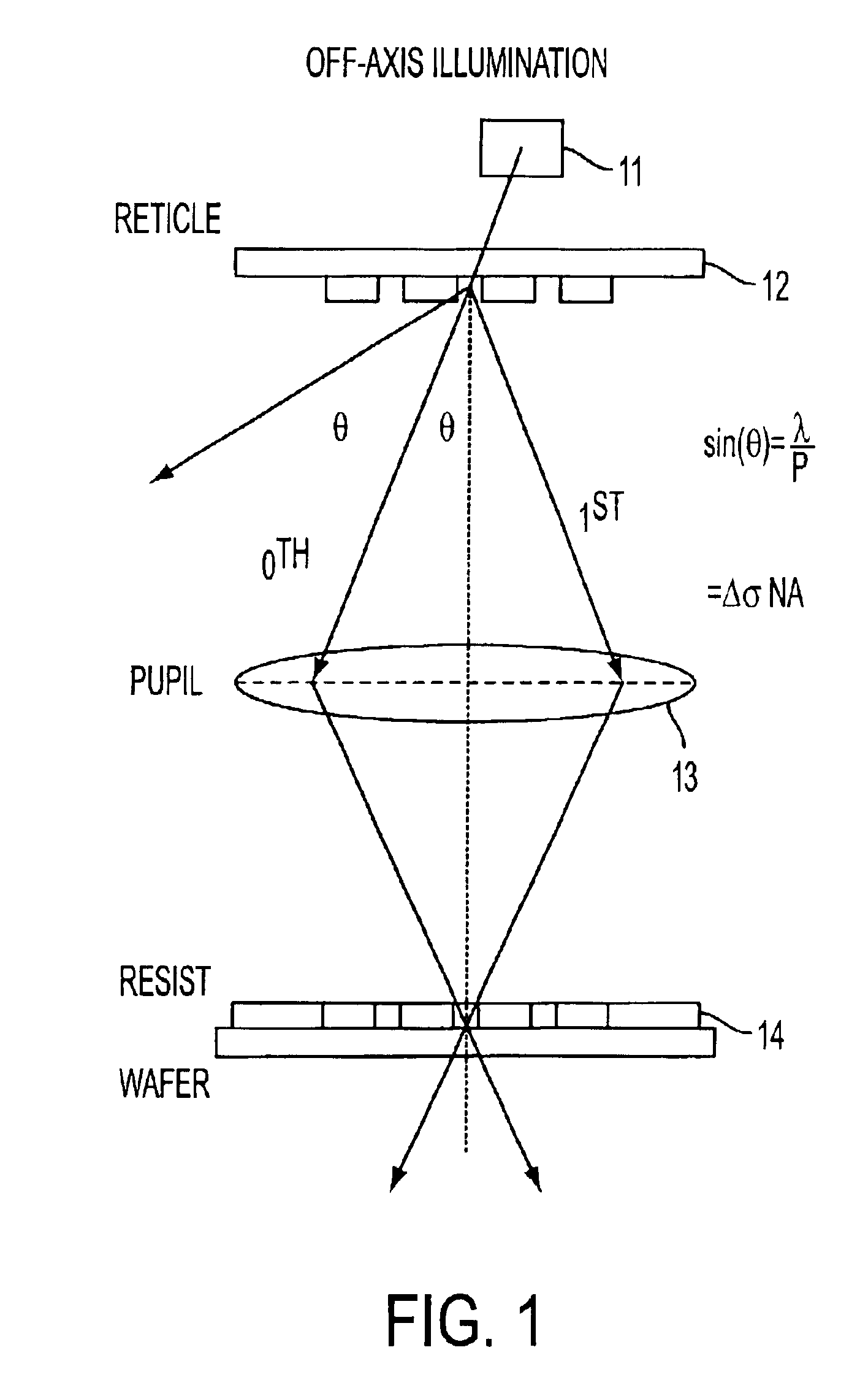
[0039]As explained in more detail below, the preferred embodiment of the present invention utilizes dipole illumination, which is an off-axis illumination (OAI) technique, in combination with a gate shrink technique in order to reduce the gate length of the transistors contained in the semiconductor device to be printed on a substrate. FIG. 1 illustrates the concept of off-axis illumination. As shown, increased focus latitude and image contrast are achieved by capturing at least one of the first orders of the pattern spatial frequencies. A typical off-axis illumination system includes in-part a light source 11, a mask 12, a lens 13 and the wafer 14 covered with photoresist.

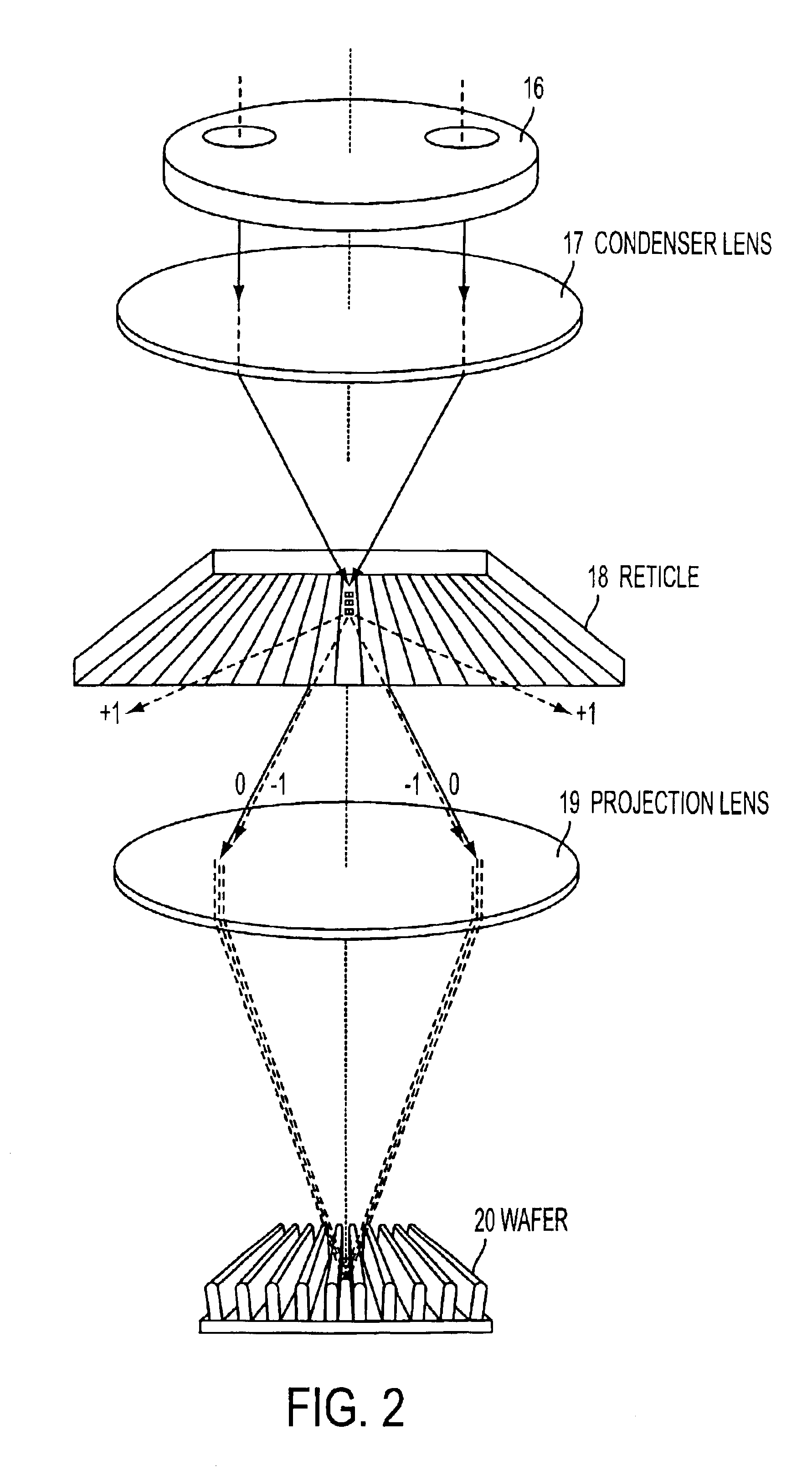
[0040]FIG. 2 illustrates the basic principles of dipole illumination. As is known, the light source is confined to two poles in order to create the conditions for two-beam imaging with theoretical infinite contrast. Referring to the example set forth in FIG. 2, the dipole illumination system includes in-part a dip...


PUM

PropertyMeasurementUnit
wavelengthaaaaaaaaaa

Abstract

A method of printing a gate pattern on a substrate comprising the steps of: identifying at least one area in the pattern in which one of the gate features overlays one of the active regions; reducing a width dimension of the one of the gate features at the location which the one of the gate features overlays the one of the active regions; extracting the gate features from the pattern; decomposing the gate features into a vertical component mask and a horizontal component mask; and illuminating the vertical component mask and the horizontal component mask utilizing dipole illumination.

Description

[0001]This application claims priority of U.S. Provisional Patent Application No. 60 / 366,537, filed Mar. 25, 2002.FIELD OF THE INVENTION[0002]The present invention relates to photolithography, and in particular relates to the generation of mask layouts for use with dipole illumination techniques that provides for both a reduction in the miminal printable gate length of transistors and an improvement in the resulting resolution. In addition, the present invention relates to a device manufacturing method using a lithographic apparatus comprising a radiation system for providing a projection beam of radiation; a mask table for holding a mask, serving to pattern the projection beam; a substrate table for holding a substrate; and a projection system for projecting the patterned projection beam onto a target portion of the substrate.BACKGROUND OF THE INVENTION[0003]Lithographic projection apparatus (tools) can be used, for example, in the manufacture of integrated circuits (ICs). In such ...

Claims


Application Information

Patent Timeline
Patent Type & Authority Patents(United States)
IPC IPC(8): G03F1/14G03F7/20G03F1/00G03F1/36H01L21/027
CPCG03F1/144G03F1/36G03F7/701G03F7/70125G03F7/70425G03F7/70433G03F7/70441G03F7/70466G03F1/70H01L21/027
Inventor HSU, STEPHEN D.CORCORAN, NOELCHEN, JANG FUNG
Owner ASML NETHERLANDS BV
Why Eureka
Try Eureka