Strained silicon-channel MOSFET using a damascene gate process

a damascene gate and silicon channel technology, applied in the direction of semiconductor devices, basic electric elements, electrical equipment, etc., can solve the problems of high junction leakage, high junction leakage, and high cost of si/sige system mosfet process, so as to improve the transport properties of fets and reduce leakage junctions

Inactive Publication Date: 2005-07-12
INT BUSINESS MASCH CORP
View PDF3 Cites 34 Cited by
  • Summary
  • Abstract
  • Description
  • Claims
  • Application Information

AI Technical Summary

Benefits of technology

[0005]The present invention provides a novel method using a damascene-gate process to improve the transport properties of FETs through strained Si. In the inventive method, changes in mobility and FET characteristics are deliberately made in a bulk Si or silicon-on-insulator (SOI) structure through the introduction of local strain in the channel region, without introducing strain in the device source and drain junctions. The present method has the advantage of not straining the source and drain junctions resulting in very low leakage junctions and also it does not require any special substrate preparation like the case of the strained Si / relaxed SiGe system. Moreover, the method of the present invention is compatible with existing mainstream CMOS processing.
[0006]Moreover, the method of the present invention is capable of forming a localized strained Si channel while not requiring that the gate implantation be very shallow. Thus, the inventive method does not have to avoid long anneal cycles. Additionally, in the present method the source / drain implants are not carried out during the gate implantation therefore shallow source / drain junctions having a depth of about 20 nm or less are possible.
[0007]The above-mentioned objects and advantages are achieved in the present invention by forming the gate in a damascene-gate process in a gate opening by depositing amorphous silicon, i.e., a:Si, at a temperature of less than about 600° C., preferably at a temperature between 500° and 600° C. During a subsequent anneal, the a:Si is converted into a polySi gate while introducing the desired localized strain in an underlying Si region without impacting the adjoining source and drain area. Source / drain junction formation occurs after formation of the strained Si channel therefore the junctions can be very shallow.
[0015]The method above is a damascene method since the gate is formed in a gate opening. The inventive method is compatible with existing mainstream CMOS processes resulting in low cost and high production rate. The method of the present invention allows for n- or p-type devices to be formed atop the localized strain channel. This is unlike the process disclosed in K. Ota, et al., “Novel Locally Strained Channel Technique for High Performance 55 nm CMOS”, December 2002, IEDM conference where PMOS devices cannot be strained due to the lack of “heavy” implant acceptor ions to cause amorphization of the p-type gates.

Problems solved by technology

MOSFET's fabricated using the Si / SiGe system exhibit the following disadvantages: (1) High source and drain junction leakage—the FET source and drain junctions, as well as the channel region, are formed in a strained Si area resulting in high junction leakage.
(2) The Si / SiGe system MOSFET process is not compatible with mainstream CMOS fabrication techniques requiring specially prepared substrates using molecular beam epitaxy.
(3) The Si / SiGe system MOSFET process is costly with low production rate.

Method used


Image

  • Strained silicon-channel MOSFET using a damascene gate process
  • Strained silicon-channel MOSFET using a damascene gate process
  • Strained silicon-channel MOSFET using a damascene gate process

Examples


Embodiment Construction

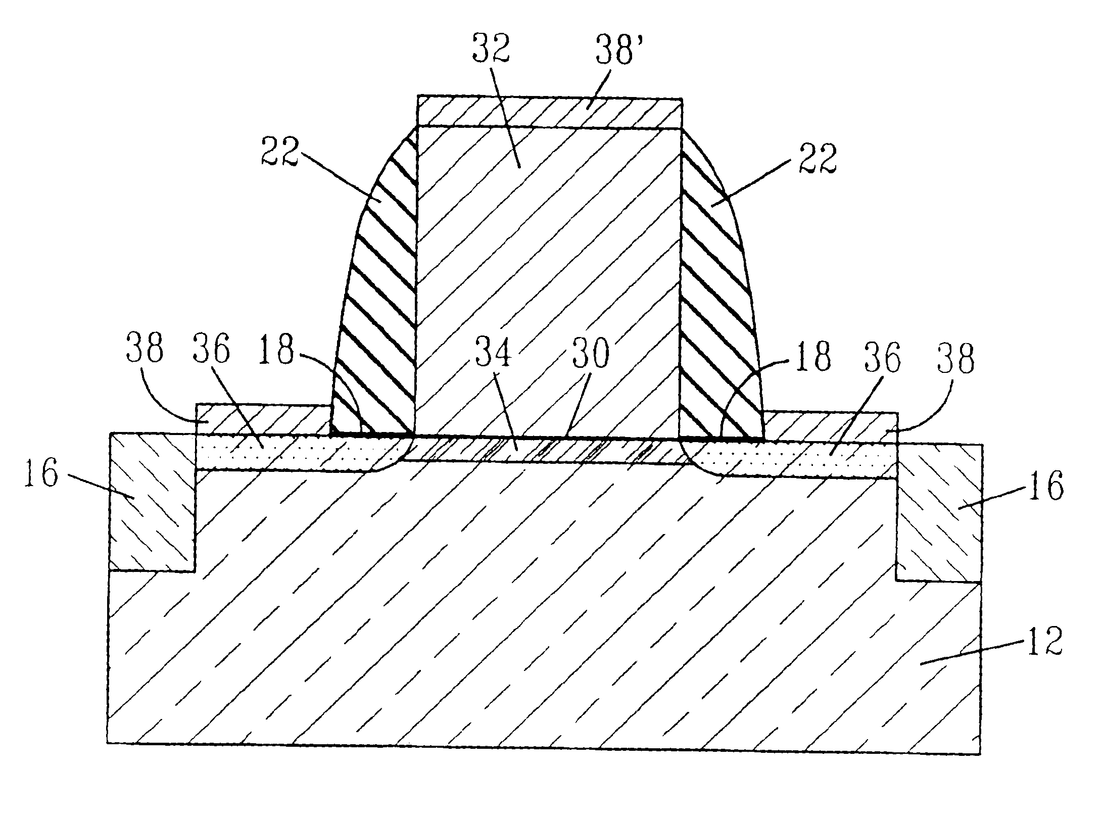
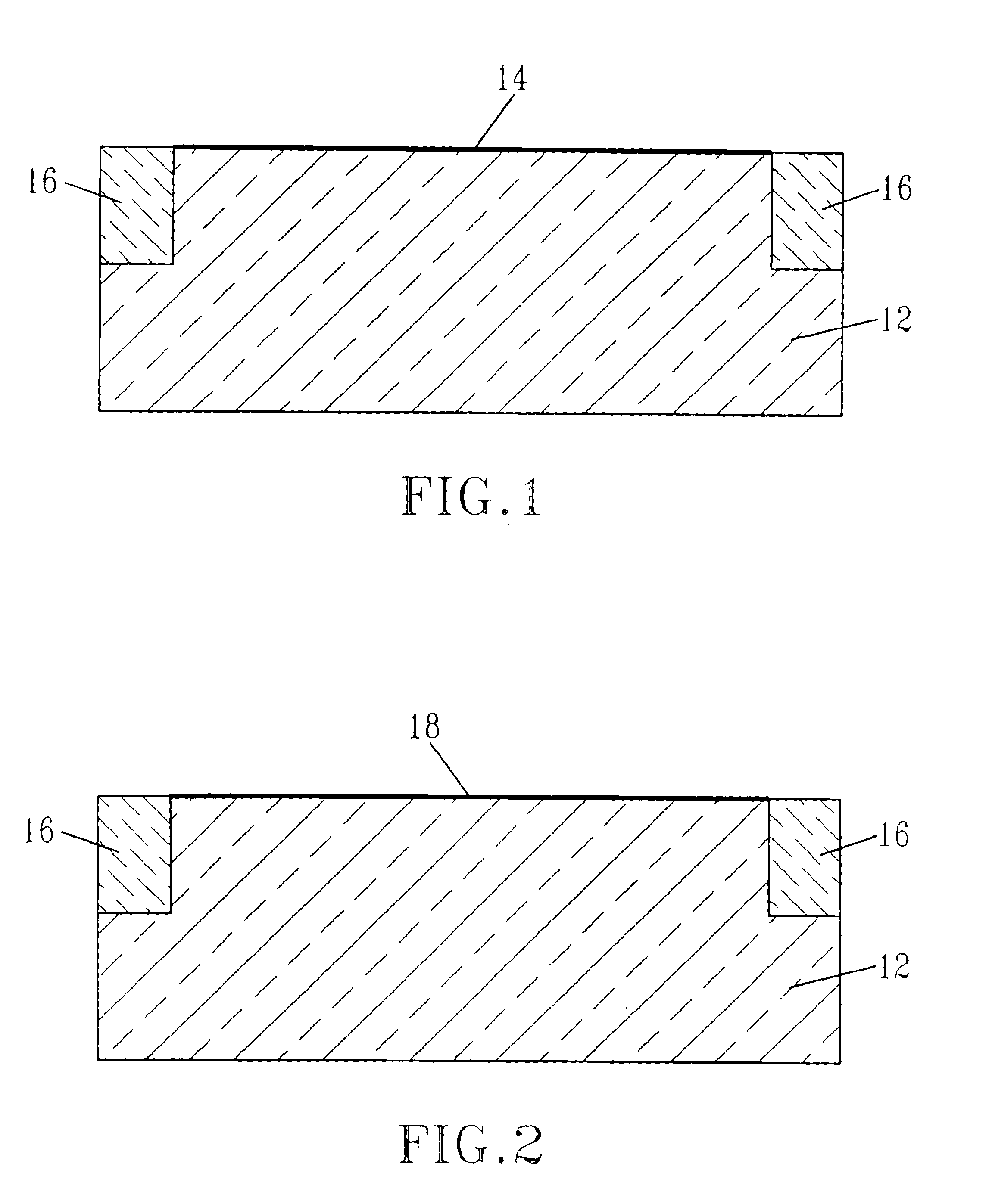
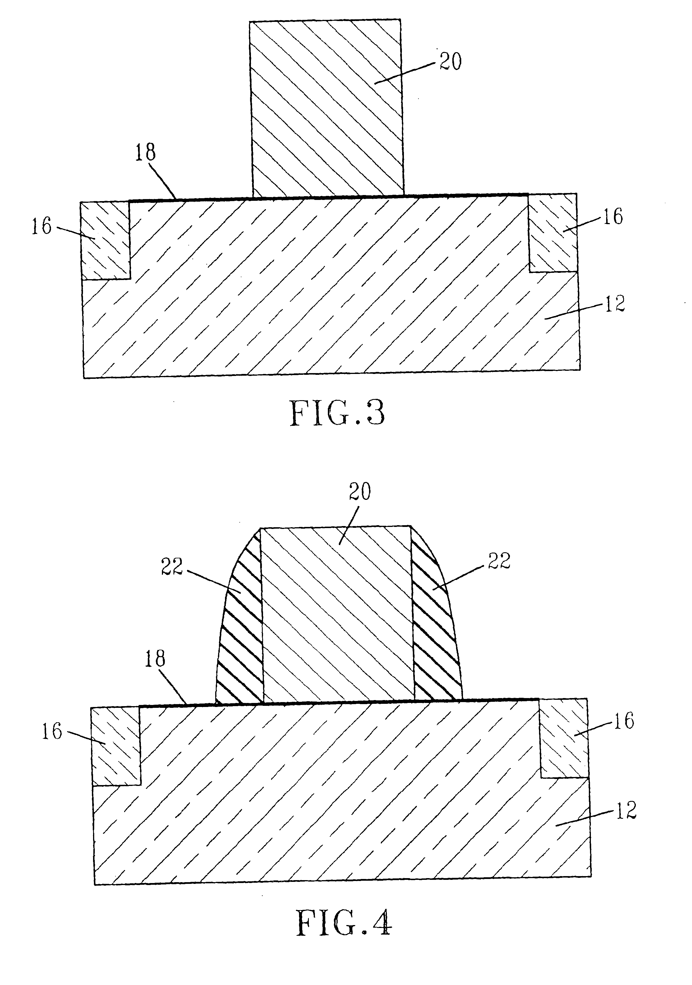
[0032]The present invention, which provides a method of fabricating local strained channel MOSFETs, will now be described in greater detail by referring to the drawings that accompany the present application. In the accompanying drawings, like and / or corresponding elements are referred to by like reference numerals.

[0033]Reference is first made to FIG. 1 that illustrates an initial structure 10 that can be employed in the present invention. Specifically, the initial structure 10 shown in FIG. 1 comprises a Si-containing semiconductor substrate or wafer 12 having trench isolation regions 16 formed therein and a pad oxide layer 14 located on surface portions of the Si-containing semiconductor substrate 12.

[0034]The term “Si-containing semiconductor substrate” denotes any semiconductor material that includes at least silicon. Illustrative examples of Si-containing semiconductor materials that can be used as substrate 12 include, but are not limited to: Si, SiGe, SiC, SiGeC, silicon-on-...


PUM


Abstract

The present invention provides a method using a damascene-gate process to improve the transport properties of FETs through strain Si. Changes in mobility and FET characteristics are deliberately made in a Si or silicon-on-insulator (SOI) structure through the introduction of local strain in the channel region, without introducing strain in the device source and drain regions. The method has the advantage of not straining the source and drain regions resulting in very low leakage junctions and also it does not require any special substrate preparation like the case of a strained Si / relaxed SiGe system. Moreover, the method is compatible with existing mainstream CMOS processing. The present invention also provides a CMOS device that has a localized strained Si channel that is formed using the method of the present invention.

Description

FIELD OF THE INVENTION[0001]The present invention relates to semiconductor device manufacturing, and more particularly to a method of fabricating a metal oxide semiconductor field effect transistor (MOSFET) device having a Si channel region that is strained and adjoining source / drain junctions that are unstrained. The method of the present invention provides MOSFET devices having a very high channel carrier mobility, while maintaining a very low leakage junction.BACKGROUND OF THE INVENTION[0002]Improvements in transport properties, i.e., carrier mobility, through strain have been demonstrated in the operating characteristics of field effect transistors (FETs). For complementary metal oxide semiconductor (CMOS) devices, an improvement in device characteristics through enhanced carrier mobility has significant potential for the fabrication of very high-speed devices. Strained silicon on a relaxed SiGe substrate is one system where such an improvement occurs, see, for example, D. K. Na...

Claims


Application Information

Patent Timeline
Patent Type & Authority Patents(United States)
IPC IPC(8): H01L21/336
CPCH01L29/665H01L29/66537H01L29/66545H01L29/7842Y10S438/938
Inventor HANAFI, HUSSEIN I.FRANK, DAVID J.CHAN, KEVIN K.
Owner INT BUSINESS MASCH CORP
Why Eureka
Try Eureka