Cathode panel for a cold cathode field emission display and cold cathode field emission display, and method of producing cathode panel for a cold cathode field emission display

a cathode panel and field emission display technology, applied in the field of cathode panels, can solve the problems of short-circuited field emission devices that cannot perform complete display, field emission devices liable to have particle defects, and field emission devices with short-circuited field emission devices

Inactive Publication Date: 2005-07-12
SONY CORP
View PDF3 Cites 13 Cited by
  • Summary
  • Abstract
  • Description
  • Claims
  • Application Information

AI Technical Summary

Benefits of technology

[0019]It is therefore an object of the present invention to provide a cathode panel for a cold cathode field emission display, which permits exclusion of a cold cathode electron emitting portion in operation or permits inhibition of operation of defective part of the cold cathode electron emitting portions when the cold cathode electron emitting portion causes a defect, and which does not incur a decrease in the production yield of cold cathode field emission displays.
[0200]In the cathode panels according to the second, fourth and sixth aspects of the present invention, in the production methods according to the second, fourth and sixth aspects of the present invention, and further in the cold cathode field emission displays according to the second, fourth and sixth aspects of the present invention, the branch wiring is preferably made of an aluminum layer or an aluminum alloy layer, or it is preferably constituted of a first branch wiring portion made of an aluminum layer or an aluminum alloy layer and a second branch wiring portion having a two-layered structure of an aluminum layer or an aluminum alloy layer and a barrier metal layer thereon, from the viewpoint of reliably breaking the branch wiring by a current flowing in the branch wiring. The aluminum layer is preferably composed of aluminum having a purity of at least 99%. The aluminum alloy layer includes Al—Si, Al—Cu and Al—Si—Cu layers. Preferably, the aluminum alloy layer contains Si and / or Cu in a total amount of 1 to 2 atomic %. The material for constituting the barrier metal is required to be a material having a higher melting point than aluminum or the aluminum alloy, and it can be selected from refractory metal such as tungsten (W), molybdenum (Mo) and titanium (Ti), nitrides such as TiN, alloys such as Ti—W, and alloys and compounds of the above refractory metal. For easily breaking the branch wiring, preferably, the branch wiring has a portion having a width of 0.5 to 5 μm, and the length of the branch wiring is at least 10 μm but does not exceed, for example 0.5 mm, although the above width and length shall not be limited thereto.

Problems solved by technology

In the steps of producing the above Spindt type field emission devices, however, it is required to peel off the peeling-off layer 57 all over the large-area support (for example, glass substrate) for producing a display having a large-area screen, and the peeling of the peeling-off layer 57 causes a defect on the field emission devices.
In a dry process, further, a reaction product is increasingly deposited in processing the large-area support, and the field emission devices are liable to have a defect due to particles.
When a short circuit is formed in the field emission device, there are some cases where the whole of one column of the stripe-shaped electron emitting portions including the short-circuited field emission device can no longer perform complete displaying.
When a field emission device is in a short-circuited state, a leak current consequently flows between the gate electrode 54 and the cathode electrode 52 through the electron emitting electrode 56 and the resistance layer, which leads to an increase in consumption power.
Another problem with the field emission devices is that the field emission devices vary in electron emitting characteristics.
As a result, there is caused a problem that a bright spot appears on a display screen.

Method used


Image

  • Cathode panel for a cold cathode field emission display and cold cathode field emission display, and method of producing cathode panel for a cold cathode field emission display
  • Cathode panel for a cold cathode field emission display and cold cathode field emission display, and method of producing cathode panel for a cold cathode field emission display
  • Cathode panel for a cold cathode field emission display and cold cathode field emission display, and method of producing cathode panel for a cold cathode field emission display

Examples


example 1

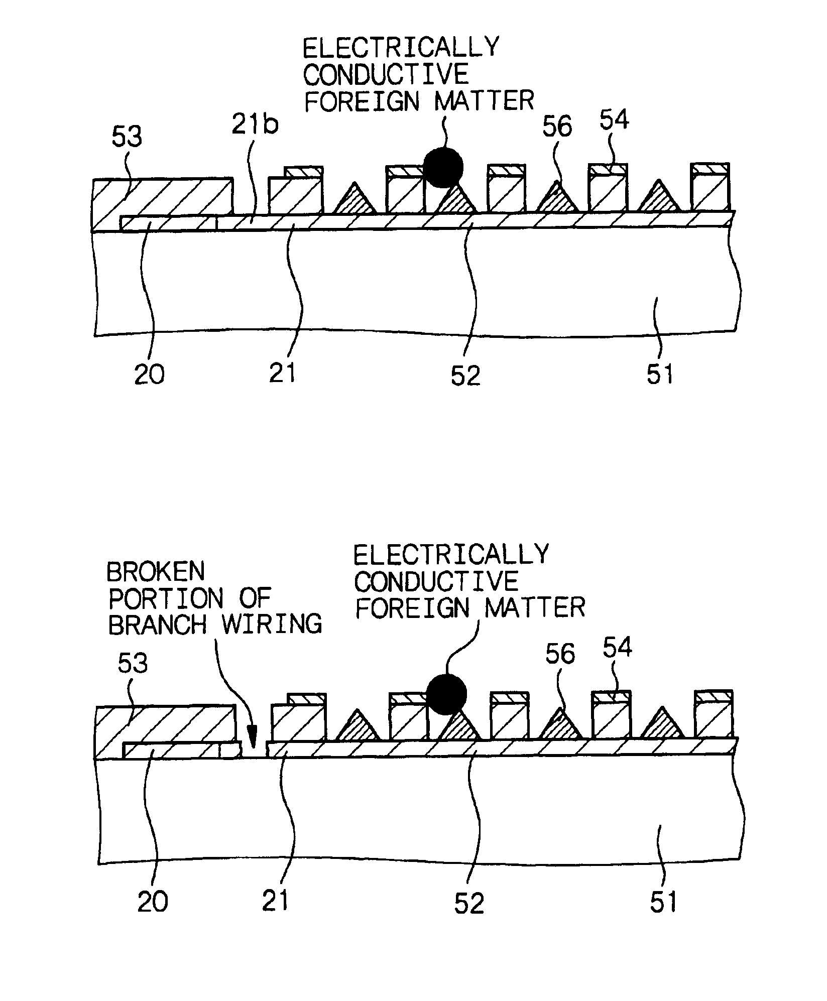
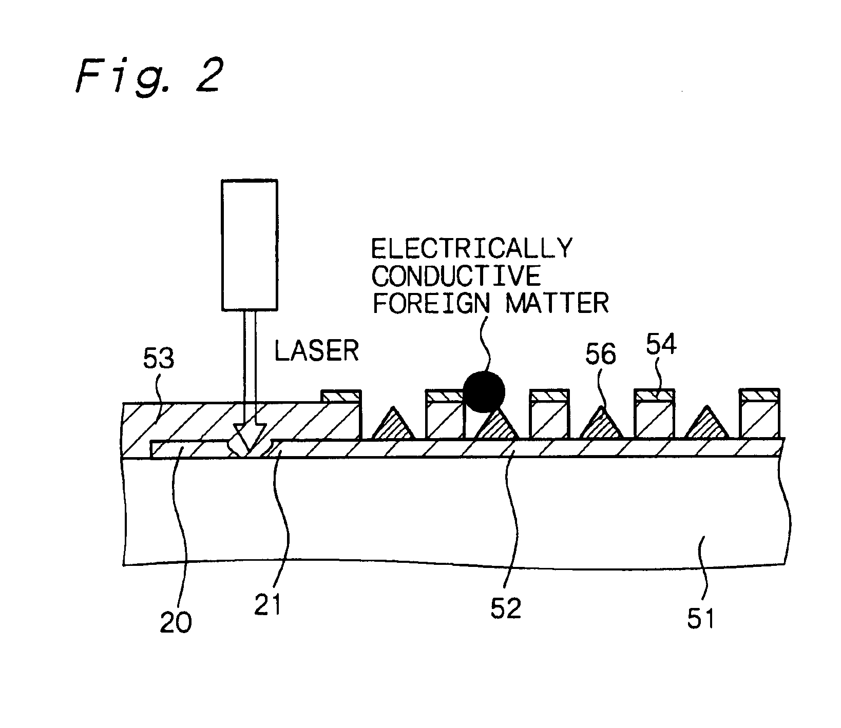
[0313]Example 1 is concerned with the cathode panel for a cold cathode field emission display (to be simply referred to as “cathode panel” hereinafter) and a display according to the first aspect of the present invention, and a method of producing the cathode panel.

[0314]The electron emitting portion 10 can be constituted of a plurality (for example, approximately tens to one thousand) of the above Spindt type field emission devices, a plurality (approximately tens to hundreds) of the above edge type field emission devices or one or a plurality of the above flat type field emission device(s). In principle, all of Examples to be described hereinafter will explain cathode panels with reference to embodiments in which the electron emitting portion 10 is constituted of a plurality of the Spindt type field emission devices, while these Examples can also apply to embodiments in which the electron emitting portion 10 is constituted of field emission devices of any other type.

[0315]As FIG. ...

example 2

[0351]Example 2 is concerned with the cathode panel, the display and the cathode panel production method according to the second aspect of the present invention.

[0352]Each of electron emitting portions can be constituted of a plurality (for example, tens to one thousand) of the Spindt type field emission devices, a plurality (approximately tens to hundreds) of the edge type field emission devices or one or a plurality of the flat type field emission device(s) which have been already explained. A cathode panel will be explained with reference to an embodiment in which each electron emitting portion is constituted of a plurality of the Spindt type field emission devices hereinafter, while the explanation can also apply to embodiments in which each electron emitting portion is constituted of field emission devices of any other type.

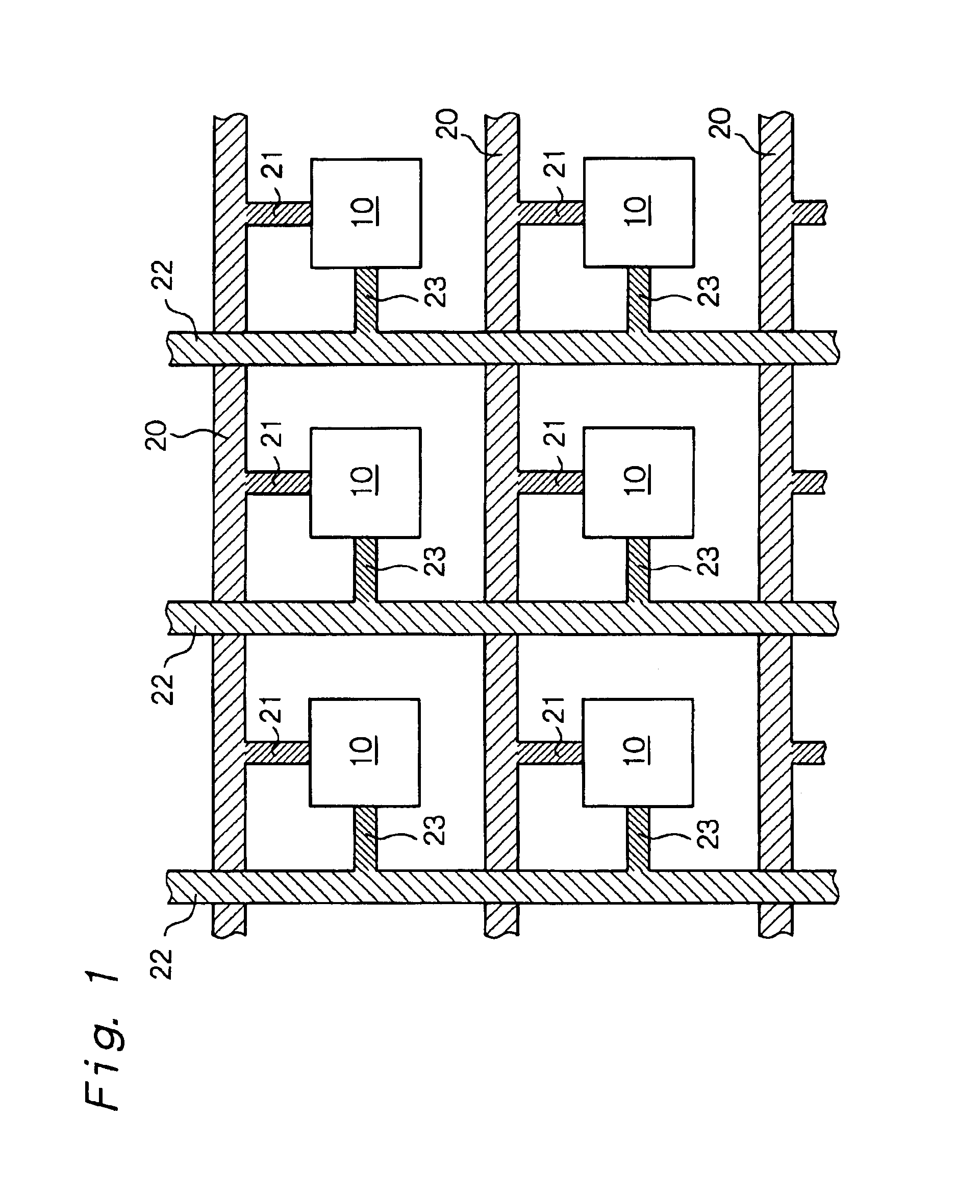
[0353]As is shown in the schematic plan layout of FIG. 6, the cathode panel of Example 2 also has a plurality of main wirings 20 and 22 (FIG. 6 shows one ea...

example 3

[0371]Example 3 is concerned with the cathode panel, the display and the cathode panel production method according to the third aspect of the present invention.

[0372]Each of electron emitting portions can be constituted of a plurality (for example, tens to one thousand) of the Spindt type field emission devices, a plurality (approximately tens to hundreds) of the edge type field emission devices or one or a plurality of the flat type field emission device(s) which have been already explained. A cathode panel will be explained with reference to an embodiment in which each electron emitting portion is constituted of a plurality of the Spindt type field emission devices hereinafter, while the explanation can also apply to embodiments in which each electron emitting portion is constituted of field emission devices of any other type.

[0373]As FIG. 3 shows the schematic plan layout of main wirings, branch wirings and electron emitting portions, the cathode panel of Example 3 has a pluralit...


PUM


Abstract

A cathode panel for a cold cathode field emission display, comprising; (a) a plurality of main wirings, (b) a plurality of branch wirings extending from each main wiring, and (c) cold cathode electron emitting portions connected to the branch wirings, wherein a branch wiring connecting a cold cathode electron emitting portion defective in operation and a main wiring is cut off.

Description

BACKGROUND OF THE INVENTION AND RELATED ART STATEMENT[0001]The present invention relates to a cathode panel for a cold cathode field emission display, a cold cathode field emission display into which the above cathode panel for a cold cathode field emission display is incorporated, and a method of producing a cathode panel for a cold cathode field emission display.[0002]Studies of various flat panel type displays are under way as displays which are to replace currently main-stream cathode ray tubes (CRT). The flat panel type displays include a liquid crystal display (LCD), an electroluminescence display (ELD) and a plasma display panel (PDP). Further, there is also proposed a cold cathode field emission display (FED), which is capable of emitting electrons into vacuum from a solid without relying on thermal excitation, and it is of great interest from the viewpoint of a high resolution, display of high-brightness colors and a low power consumption.[0003]A cold cathode field emission...

Claims


Application Information

Patent Timeline
Patent Type & Authority Patents(United States)
IPC IPC(8): H01J29/00H01J29/92H01J1/304H01J1/30H01J9/42H01J9/02H01J9/50H01J29/04H01J31/12
CPCH01J1/3042H01J9/025H01J9/50H01J29/04H01J31/127H01J2201/319H01J2329/0494Y02W30/82G09G3/22H01J1/30H01J9/02
Inventor KAMIDE, YUKIHIROKUBOTA, SHINJISATA, HIROSHIKIKUCHI, KAZUO
Owner SONY CORP
Why Eureka
Try Eureka