Wafer probe station

a technology of wafer probe station and wafer body, which is applied in the direction of individual semiconductor device testing, printed circuit testing, instruments, etc., can solve the problems of adversely affecting low level voltage and current measurement, and mechanisms that often perturb measurements taken in integrated circuit device requiring very low level measurement, so as to improve performance and low noise

Inactive Publication Date: 2005-07-12
SILICON VALLEY BANK
View PDF3 Cites 61 Cited by
  • Summary
  • Abstract
  • Description
  • Claims
  • Application Information

AI Technical Summary

Benefits of technology

[0009]The present invention addresses the problems associated with prior art probe stations by providing an integrated guarding and shielding approach for limiting electrical leakage currents and noise. The guarding and shielding system provides a line-of-sight electrical barrier between a shielding element and the conductive wafer support layer to both minimize leakage currents, parasitic capacitance, electromagnetic interference (EMI) and other noise sources.
[0012]The insulator supported on the lower chuck element may be provided in various geometric configurations to permit a number of arrangements of the conductive test layer, the peripheral conductive element and the lower chuck element relative to each other. The unique design is mechanically rigid, ensures proper registration of the various components over time, and provides improved performance in low voltage and low noise applications. The novel chuck assembly of the invention may be arranged in a variety of electrical connection schemes with the test instrumentation and with the probe station chassis.

Problems solved by technology

Decreasing the scale of the circuit can provide the aforementioned improvements, however, tradeoffs in performance may also occur.
A number of factors can adversely affect low level voltage and current measurements, including, impedances in which an impedance or current path unintentionally shares a noise source or other instrumentation, the transfer of a noise voltage through usually coupled incidental inductances, magnetically coupled noise, incidental capacitive coupling, charge transfer due to the proximity of charge bodies to the test circuitry, and the like.
These mechanisms often perturb measurements taken in integrated circuit devices requiring very low level measurements.
The measurement of current values in the high attoampere and the low femtoampere regime is particularly difficult in the presence of interfering sources that may be capable of generating current flow of electrons which, though minuscule, may be substantial relative to the very low voltage and low currents being measured.
The size of the annular space provided in such a design directly affects its dielectric properties and capacitance, and in turn the degree of isolation from the support surface on which testing occurs.
However, maintaining the desired registration between the chuck elements and the guard ring in such a design may be difficult.
Even slight offsets in the associated mechanical connections between the various elements or in the shape of the guard ring can affect the registration and detrimentally alter the performance of the chuck.
Such an approach may be suitable in certain applications, but does not provide significant guarding around the side periphery of the conductive support surface and the location of testing.
In addition, with the annular side wall of the shield opposing the metal sputtered insulator element, parasitic and parallel capacitance may occur between the shield and the conductive test surface and distort test measurements.
It would be desirable therefore to provide an integrated approach to guard and shield systems of wafer probe stations designed to accommodate low level current and voltage measurements with sensitivities in the high attoampere and the low femtoampere regime, which is not easily feasible with presently known designs of guarding systems or shielding systems in commercial probe stations.
Measurements of low level currents in the high attoampere and low femtoampere regime are particularly susceptible to errors induced by capacitive loading, electrical discharge, and noise events which occur because of the dielectric characteristics of nonconductors in and surrounding the conductive test surface, which effects may significantly distort measurement values and limit the accuracy of low voltage and low current measurements.
Poor tester and prober grounding or poorly insulated or guarded probes will contribute to electrical noise from power supplies or external circuits which may enter the probing environment and be coupled to the measurements.

Method used


Image

  • Wafer probe station
  • Wafer probe station
  • Wafer probe station

Examples


Embodiment Construction

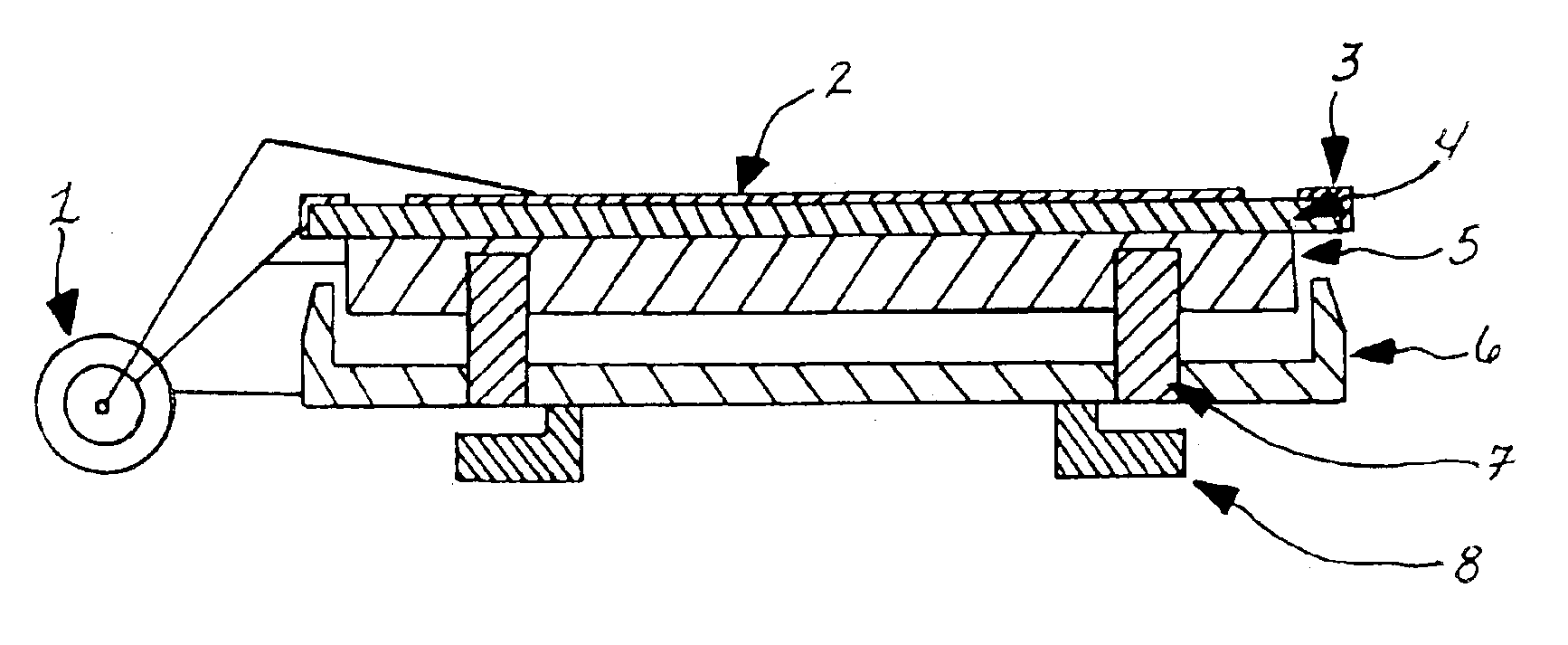
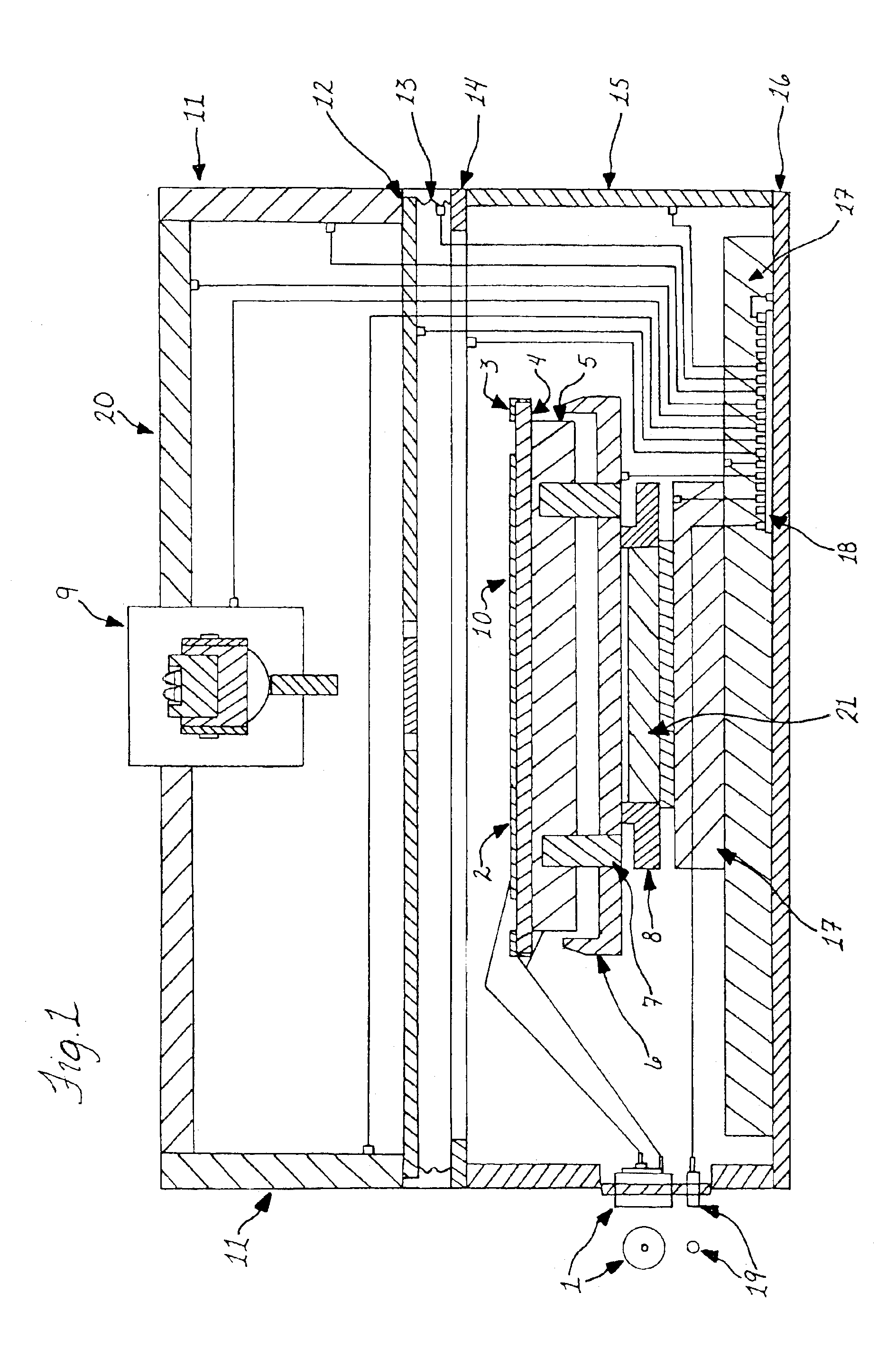
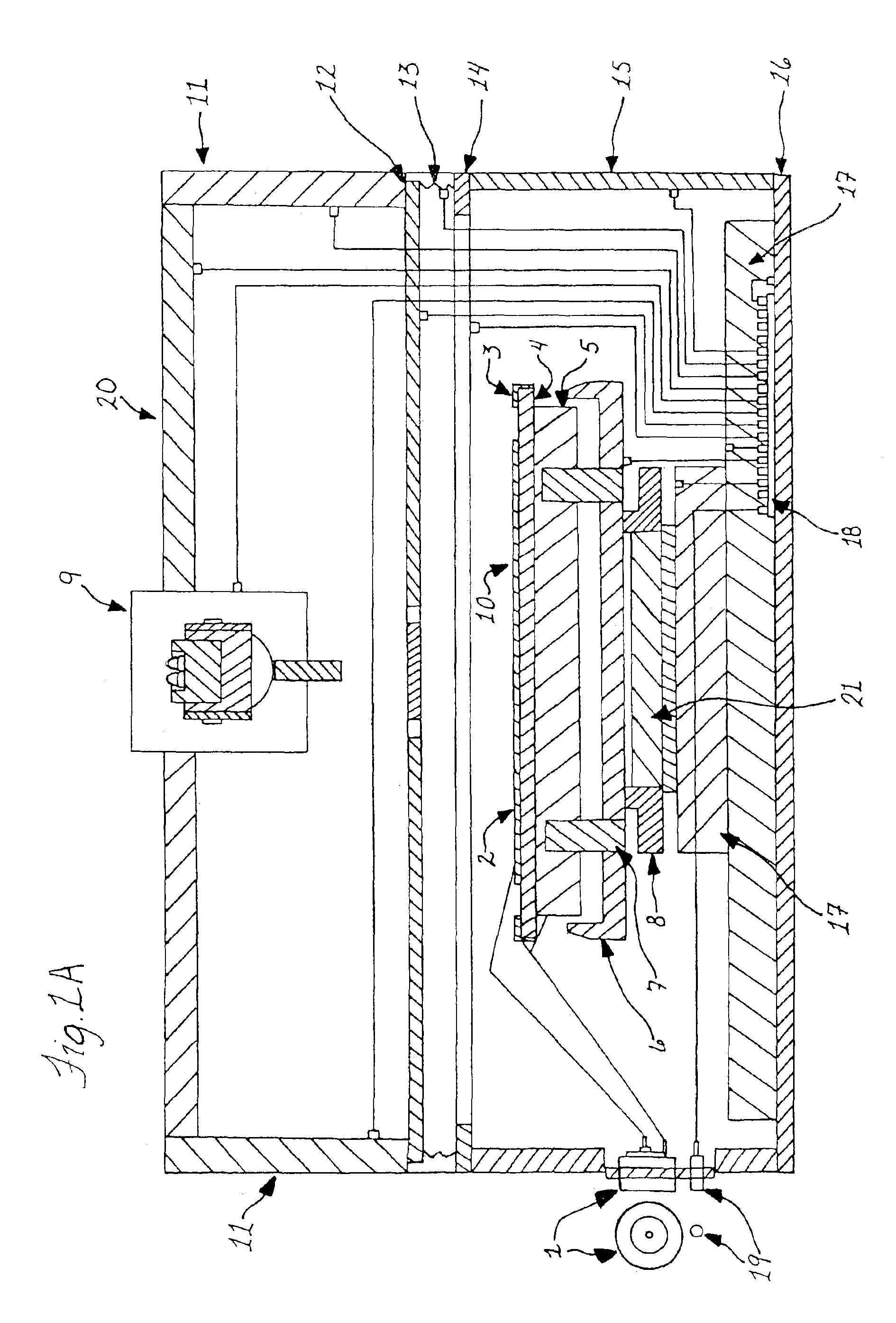
[0030]With reference to FIG. 1, a wafer probe station embodiment is shown in which a chuck apparatus 10 is supported within a probe station chassis. The chuck apparatus supports a wafer or other semiconductor integrated circuit device under test (DUT). The chuck apparatus 10 may be independently moved along X and Y axes using a positioner (not shown), which controls the X and Y components of the stage 17. The chuck apparatus 10 is positioned on a hub 21, which is attached to the X / Y stage construction 17 of the wafer probe station. As shown, a coaxial connection 1 is indicated for electrical signals being provided to the wafer probe station. Another connection 19 is provided to facilitate grounding of the probe station chassis by means of central point ground 18. As shown in FIG. 1A, a triaxial connection implementation may also be provided for the electrical signals, e.g., force, guard, and sense, that are applied at the wafer probe station to facilitate grounding of triaxial cable...


PUM


Abstract

The invention relates to a chuck apparatus for a wafer probe station in which the central conductive surface supports a device-under-test (DUT) over a conductive lower chuck portion. An insulator positions the center conductor surface of the chuck above the lower chuck portion and also positions an electrically isolated conductor along its periphery. A laterally extending shielding element is provided for shielding electromagnetic interference (EMI) from the center conductor surface and the lower chuck portion. The electrically isolated conductor and the conductive lower chuck portion may cooperate to form a line-of-sight electrical barrier between the center conductor surface and the laterally extending shielding element. The invention further relates to methods of manufacturing the chuck apparatus and using the apparatus to accomplish low current and voltage tests in a probe station.

Description

RELATED APPLICATIONS[0001]This is a division of prior application Ser. No. 10 / 134,908, filed Apr. 29, 2002, U.S. Pat. No. 6,803,756 which is a division of prior application Ser. No. 09 / 615,454, filed Jul. 13, 2000, now issued as U.S. Pat. No. 6,424,141, which are hereby incorporated herein by reference in their entirety.BACKGROUND OF THE INVENTION[0002]The present invention relates to an apparatus and method of manufacture for wafer probe station systems and the use of guarding and shielding systems for limiting electrical leakage currents and noise. More particularly, the invention relates to approaches for providing a chuck apparatus system which facilitates guarding and shielding techniques for improving the accuracy of low current and low voltage measurements of a device-under-test (DUT), typically a wafer containing one or more integrated circuits.[0003]Modern wafer probe stations have been developed for making accurate low voltage and low current measurements of semiconductor ...

Claims


Application Information

Patent Timeline
Patent Type & Authority Patents(United States)
IPC IPC(8): G01R31/28G01R1/02G01R1/18
CPCG01R1/18G01R31/281G01R31/2851G01R31/2886G01R1/025G01R31/2889
Inventor HOLLMAN, KENNETH F.
Owner SILICON VALLEY BANK
Why Eureka
Try Eureka