Direct write lithography system

a lithography system and write-in technology, applied in the field of write-in lithography systems, can solve the problems of system drawbacks, very difficult to produce masks, and very slow system using raster scanning methods, and achieve the effect of easy production

Inactive Publication Date: 2005-07-19
ASML NETHERLANDS BV
View PDF10 Cites 36 Cited by
  • Summary
  • Abstract
  • Description
  • Claims
  • Application Information

AI Technical Summary

Benefits of technology

[0025]In another embodiment of the invention, the plane of the electron sources is imaged onto the object with a set of conventional electron lenses as if the electron beams were one single beam. The plane with electron sources may be imaged with a magnification of 1

Problems solved by technology

Due to the fact that these systems are all optical, the resolution is limited.
The system, however, has its drawbacks.
First, the details on the mask have to be very small, about 100 nm, making these masks very difficult to produce.
Such a system using raster scanning method is very slow.
Still this system is not fast enough for transferring an entire pattern onto a wafer fast enough for mass production purposes.
One disadvantage of this method is that the electron beams are very close together.
Due to aberrations of the electron lenses, a lot of distortion occurs.
Furthermore, as the beams have to be focussed, use is made of lenses causing the beams to converge at one point along the beam path, causing even more problems due to coulomb interactions.
Furthermore,

Method used


Image

  • Direct write lithography system
  • Direct write lithography system
  • Direct write lithography system

Examples


Embodiment Construction

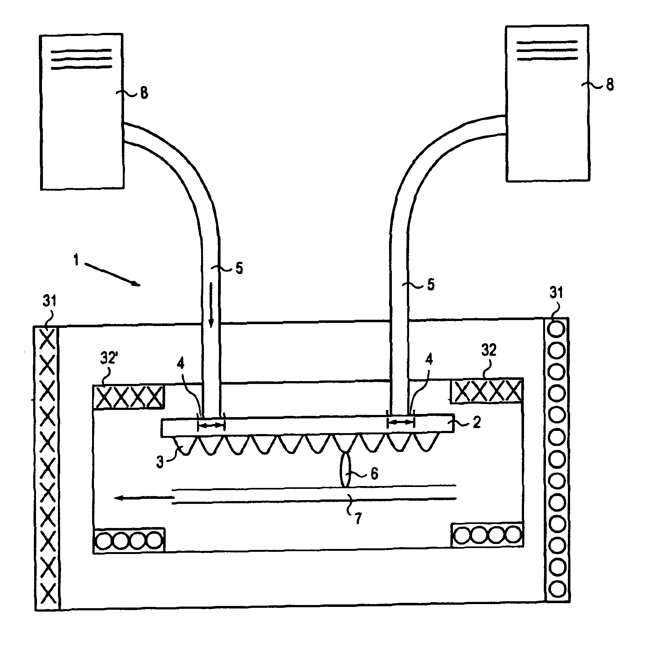
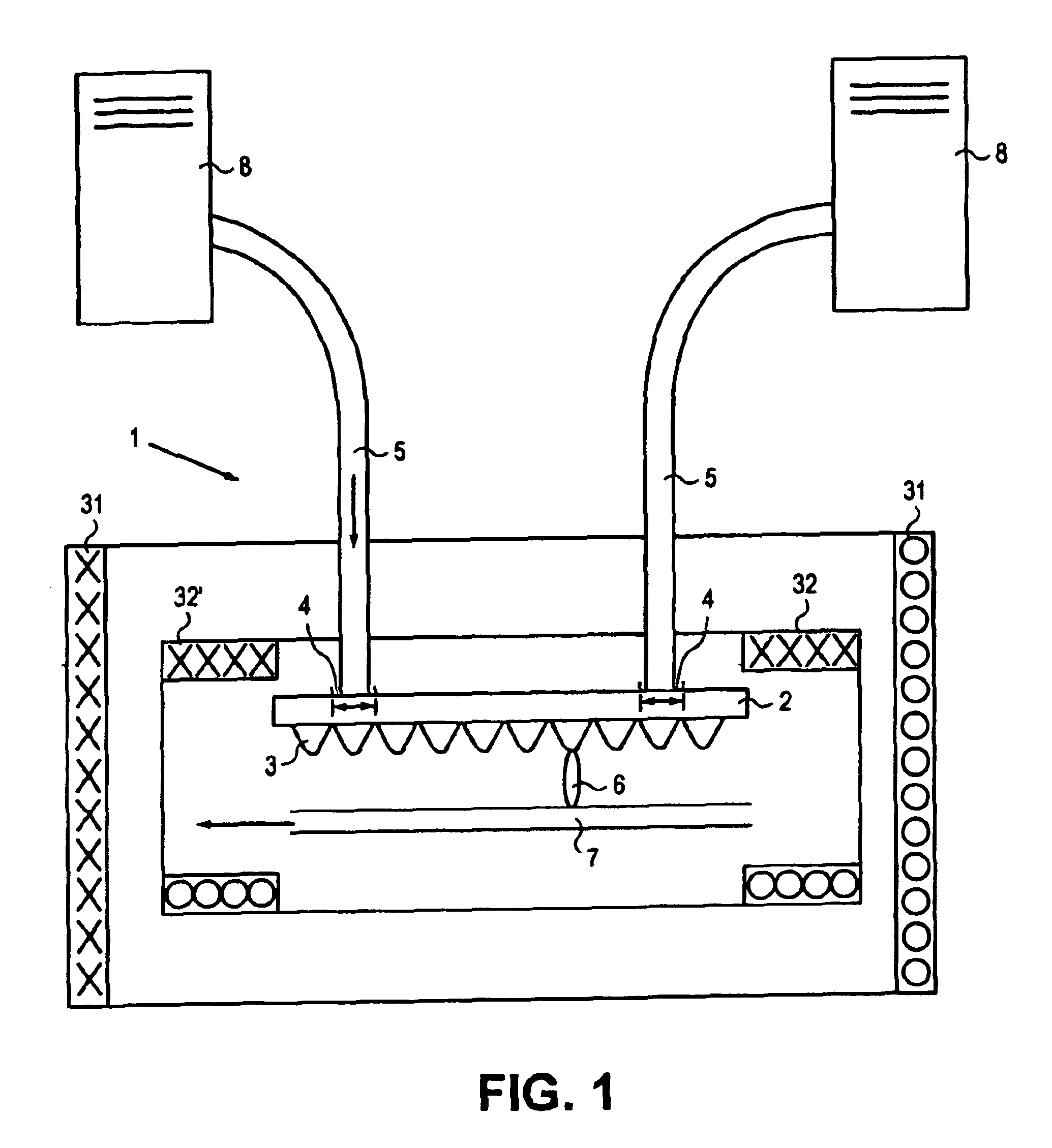
[0039]FIG. 1 shows a direct write or mask-leas lithography system 1. The system comprises converter plate 2, for instance a field emission array, in an embodiment for instance a semiconductor field emission array. Such a field emission array comprises a two-dimensional array of cathodes 3. In case the field emission array is a semiconductor field emission array, the cathodes are tips or needles of semiconductor material, like silicon tips. An example of a usable field emission array is described in PCT / NL00 / 00657 and PCT / NL00 / 00658. Each tip is capable of emitting an electron beamlet 6. Each tip has an activation area 4 on the side of the field emission array opposite to the cathodes 3. This activation area 4 is much wider than the electron beamlet 6: usually, the activation area 4 is about 2 microns wide, and the cross section of an electron beamlet is less than 100 nm, and can even be as small as 10 nm. Each electron beamlet 6 is projected onto a substrate 7, usually a semiconduct...


PUM

PropertyMeasurementUnit
Angleaaaaaaaaaa
Angleaaaaaaaaaa
Angleaaaaaaaaaa

Abstract

The mask-less lithography system has a converter that includes an array of light controllable electron sources. Each electron source is arranged for converting light into an electron beam and has an activation area. Individually controllable light sources are included where each light source is arranged for activating one electron source. A Controller controls each light source individually and each electron beam is focused on an object plane with a diameter smaller than the diameter of an individually controllable light source.

Description

[0001]This application claims the benefit of U.S. Provisional Application No. 60 / 365,843, filed Mar. 19, 2002.FIELD OF THE INVENTION[0002]The present invention relates to a mask-less or direct write lithography system.BACKGROUND[0003]Current lithography systems are mostly all optical, deep UV systems. These systems use light in the deep UV region, i.e. 193 nm. Due to the fact that these systems are all optical, the resolution is limited.[0004]One way of realising smaller resolutions is by using particle beams, especially electron beams. A known system uses masks just like all optical systems. The masks are situated between a substrate and an electron source in order to blind off parts of the electron beam. In that way, patterns are transferred to a resist. The system, however, has its drawbacks. First, the details on the mask have to be very small, about 100 nm, making these masks very difficult to produce. Furthermore, as electron beams are more energetic than light beams, the mask...

Claims


Application Information

Patent Timeline
IPC IPC(8): G03F7/20H01J37/317
CPCB82Y10/00B82Y40/00G03F7/2059G03F7/70375H01J37/3174H01J37/3177G03F7/2051Y10T428/24802H01J2237/31774H01J2237/31777H01J2237/31779Y10S438/949Y10S438/942
Inventor KRUIT, PIETER
Owner ASML NETHERLANDS BV
Why Eureka
Try Eureka