Semiconductor device and manufacturing method for the same, circuit board, and electronic device

a technology of semiconductor devices and manufacturing methods, applied in the direction of semiconductor devices, semiconductor/solid-state device details, electrical apparatus, etc., can solve the problem of not offering outstanding productivity, and achieve the effect of improving the productivity of manufacturing semiconductor devices

Inactive Publication Date: 2005-07-26
SEIKO EPSON CORP
View PDF6 Cites 45 Cited by
  • Summary
  • Abstract
  • Description
  • Claims
  • Application Information

AI Technical Summary

Benefits of technology

[0006]The present invention is directed to solving this problem and an object of the invention is

Problems solved by technology

This means that multiple individual heat sinks must be handled ind

Method used


Image

  • Semiconductor device and manufacturing method for the same, circuit board, and electronic device
  • Semiconductor device and manufacturing method for the same, circuit board, and electronic device
  • Semiconductor device and manufacturing method for the same, circuit board, and electronic device

Examples


embodiment 1

[0068

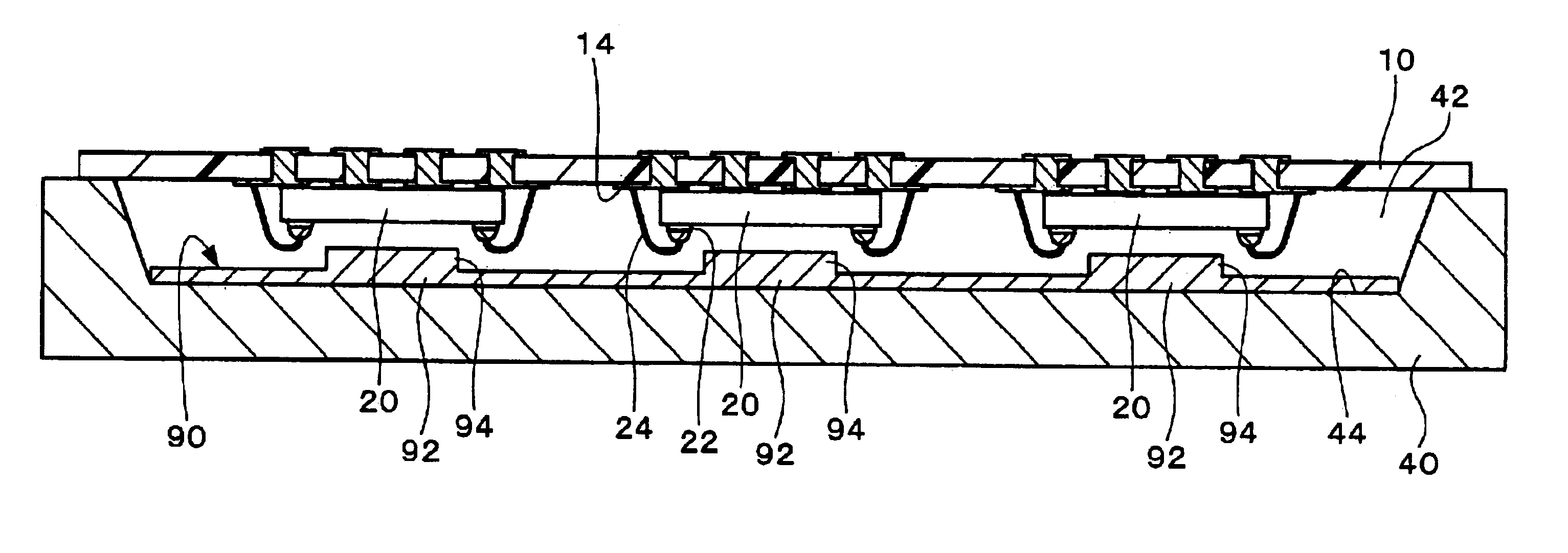
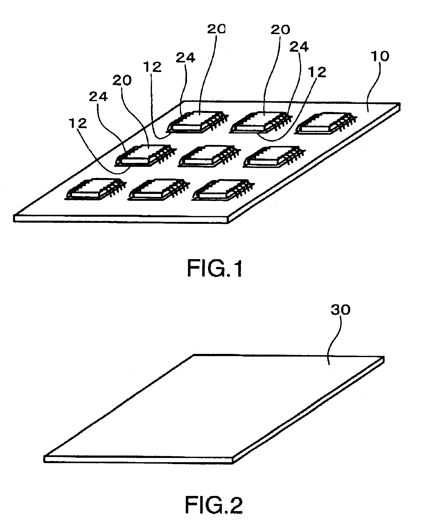
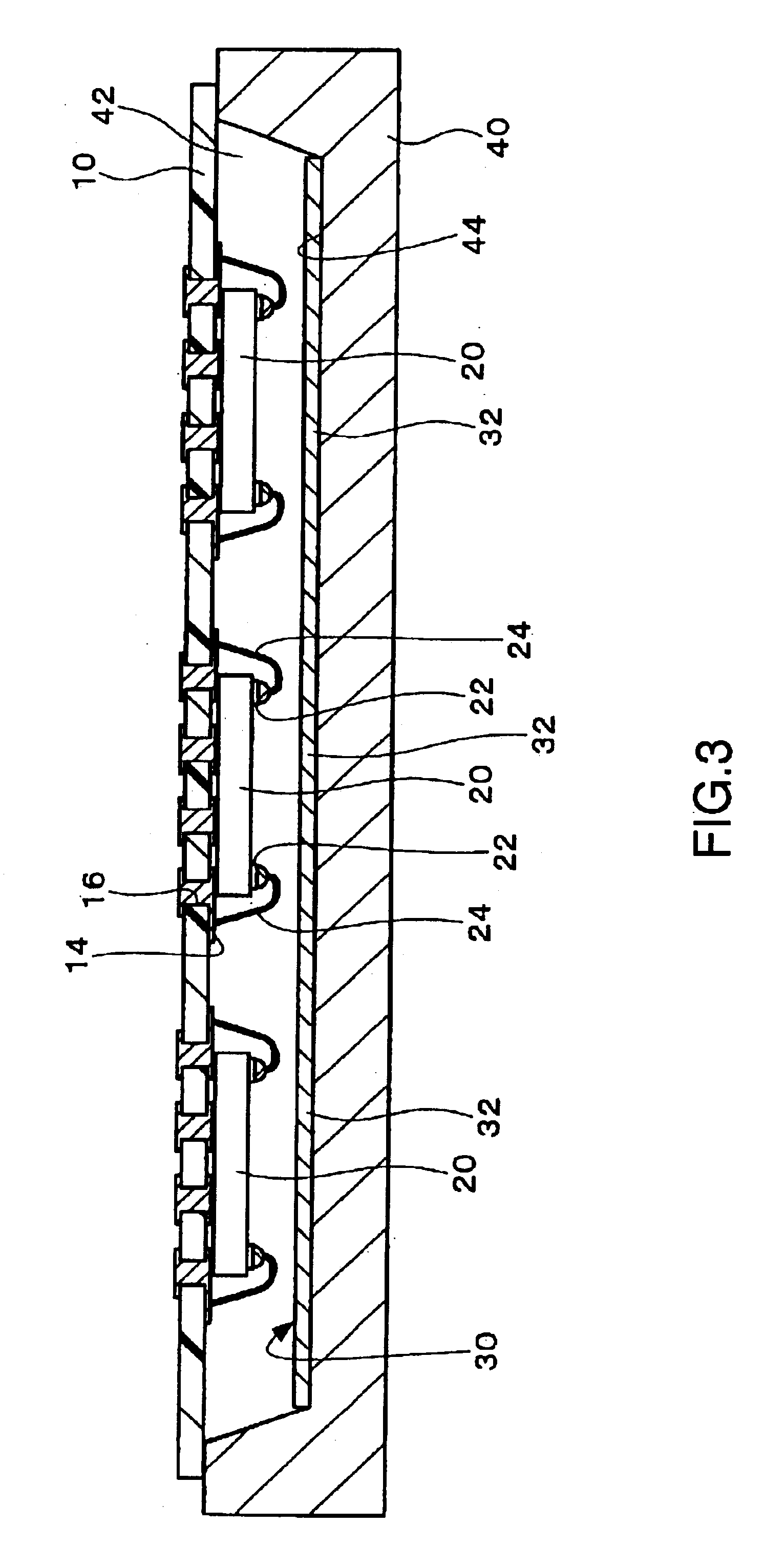
[0069]FIG. 1 to FIG. 6 show a manufacturing method for a semiconductor device according to a first embodiment of the invention. First, as shown in FIG. 1, multiple semiconductor chips 20 are mounted on a substrate 10. The substrate 10 is the interposer of the individual semiconductor devices.

[0070]The substrate 10 could be made from organic materials (such as a polyimide substrate) or inorganic materials (a ceramic or glass substrate, for example), or a hybrid (a glass-epoxy substrate, for example). The planar shape of the substrate 10 is not particularly limited but is typically rectangular as shown in FIG. 1. The substrate 10 could further be a single or multiple layer substrate.

[0071]Multiple mounting areas 12 are disposed on the substrate 10 for mounting multiple semiconductor chips 20. The mounting areas 12 are formed on either one or both sides of the substrate 10. In the example shown in FIG. 1 the multiple mounting areas 12 are formed in a matrix pattern of multiple row...

embodiment 2

[0091

[0092]FIG. 7 and FIG. 8 show a single semiconductor device according to a second embodiment of the invention. This embodiment differs from the above in the configuration of the heat sink set (shown in FIG. 7 and FIG. 8 as the heat sink after slicing). More specifically, one or both surfaces of the heat sink set are rough surfaces.

[0093]As shown in FIG. 7 the surface 64 of heat sink set 60 facing the substrate 10 can be rough. The surface 64 of heat sink set 60 can be roughened so as to remove the smoothness mechanically by sandblasting, physically using plasma, UV radiation, or ozone, for example, or chemically using an etchant. The surface could also be roughened by dimpling. It should be noted that it is sufficient to roughen the heat sink 62 part of the heat sink set 60.

[0094]With this configuration the side of the heat sink set 60 (or heat sink 62) facing the substrate 10 is the part that contacts the sealant (or sealed part 51). This increases the bonding area between the ...

embodiment 3

[0098

[0099]FIG. 9 shows a single semiconductor device according to a third embodiment of the invention. In this embodiment a plurality of through-holes 84 are formed in the heat sink set 80 (in the heat sink 82 after cutting in FIG. 9). These through-holes 84 pass through from the surface of the heat sink set 80 facing the substrate 10 to the opposite surface of the heat sink set 80, and are formed at least in the parts of the heat sink set 80 that become the heat sinks 82. The multiple through-holes 84 can be formed chemically by etching or physically or mechanically using a drill, for example.

[0100]Adhesion between the heat sink set 80 (or heat sink 82) and sealant (or sealed part 51) is improved by forming these through-holes 84 in the heat sink set 80 because the sealant also enters the through-holes 84.


PUM


Abstract

To improve the productivity of manufacturing semiconductor devices having a heat sink, the semiconductor device manufacturing method includes: (a) setting an integral heat radiation body set 30 of multiple heat radiation bodies 32 in a mold 40 cavity 42; (b) setting a substrate 10 on which multiple semiconductor chips 20 are mounted in a planar arrangement in the mold 40 so that the multiple semiconductor chips 20 are located inside the cavity 42; and (c) sealing the multiple semiconductor chips 20 and affixing the heat radiation body set 30 by filling the cavity 42 with a sealant.

Description

BACKGROUND OF THE INVENTION[0001]1. Field of the Invention[0002]The present invention relates to a semiconductor device and a manufacturing method for the same, a circuit board, and an electronic device.[0003]2. Description of the Related Art[0004]Semiconductor devices having a heat dissipating body commonly called a heat sink are known. A heat sink is disposed with at least part thereof embedded in the sealed part when the semiconductor chip is sealed. A molding process using a mold is typically used for sealing the semiconductor chip. Providing a heat sink improves the heat radiation of the semiconductor device.[0005]Conventional molding processes place one of plural heat sinks cut into individual pieces into one of the cavities used to form the sealed part. This means that multiple individual heat sinks must be handled individually, which cannot be said to offer outstanding productivity.OBJECTS OF THE INVENTION[0006]The present invention is directed to solving this problem and an...

Claims


Application Information

Patent Timeline
IPC IPC(8): H01L23/28H01L23/31H01L23/36H01L23/433H01L23/34H01L21/56H01L23/29
CPCH01L23/3128H01L23/36H01L23/4334H01L24/97H01L2224/48091H01L2224/48227H01L2224/48465H01L2224/73265H01L2224/97H01L2924/01004H01L2924/01013H01L2924/01029H01L2924/01033H01L2924/01078H01L2924/01082H01L2924/09701H01L2924/14H01L2924/15311H01L2924/19043H01L2224/85H01L2924/00014H01L2224/83H01L24/48H01L2924/01005H01L2924/01006H01L2224/32225H01L2924/1815H01L2224/73204H01L2224/16225H01L2924/00H01L2924/00012H01L2924/10253H01L2924/15787H01L2924/181H01L24/73H01L2224/05624H01L2224/05647H01L2224/45099H01L2224/85399H01L2224/45015H01L2924/207
Inventor NAKAYAMA, TOSHINORI
Owner SEIKO EPSON CORP
Why Eureka
Try Eureka