Apparatus for manufacturing GaN substrate and manufacturing method thereof

a technology of gan substrate and manufacturing method, which is applied in the direction of crystal growth process, nuclear engineering, transportation and packaging, etc., can solve the problems of cracks, gan substrate cracks, gan substrate bending, etc., and achieve the effect of preventing micro-cracks or bending of gan substra

Inactive Publication Date: 2005-08-02
LG ELECTRONICS INC
View PDF2 Cites 23 Cited by
  • Summary
  • Abstract
  • Description
  • Claims
  • Application Information

AI Technical Summary

Benefits of technology

[0011]An object of the present invention is to provide an apparatus for manufacturing GaN substrate and a manufacturing method thereof enabling to prevent micro-cracks or bending of a GaN substrate due to temperature drop by separating a substrate and a GaN layer from each other inside a chamber after growing the GaN layer on the substrate inside the chamber.

Problems solved by technology

However, the GaN substrate manufacturing method according to the related art carries out the laser lift-off process at a room temperature after growing the GaN layer at the high temperature of at least 1,000° C., whereby cracks are formed on the GaN substrate due to the abrupt temperature drop or the GaN substrate is bent.
Besides, the temperature difference between the two chambers brings about the crack or bending of the GaN substrate.

Method used


Image

  • Apparatus for manufacturing GaN substrate and manufacturing method thereof
  • Apparatus for manufacturing GaN substrate and manufacturing method thereof
  • Apparatus for manufacturing GaN substrate and manufacturing method thereof

Examples


first embodiment

[0028

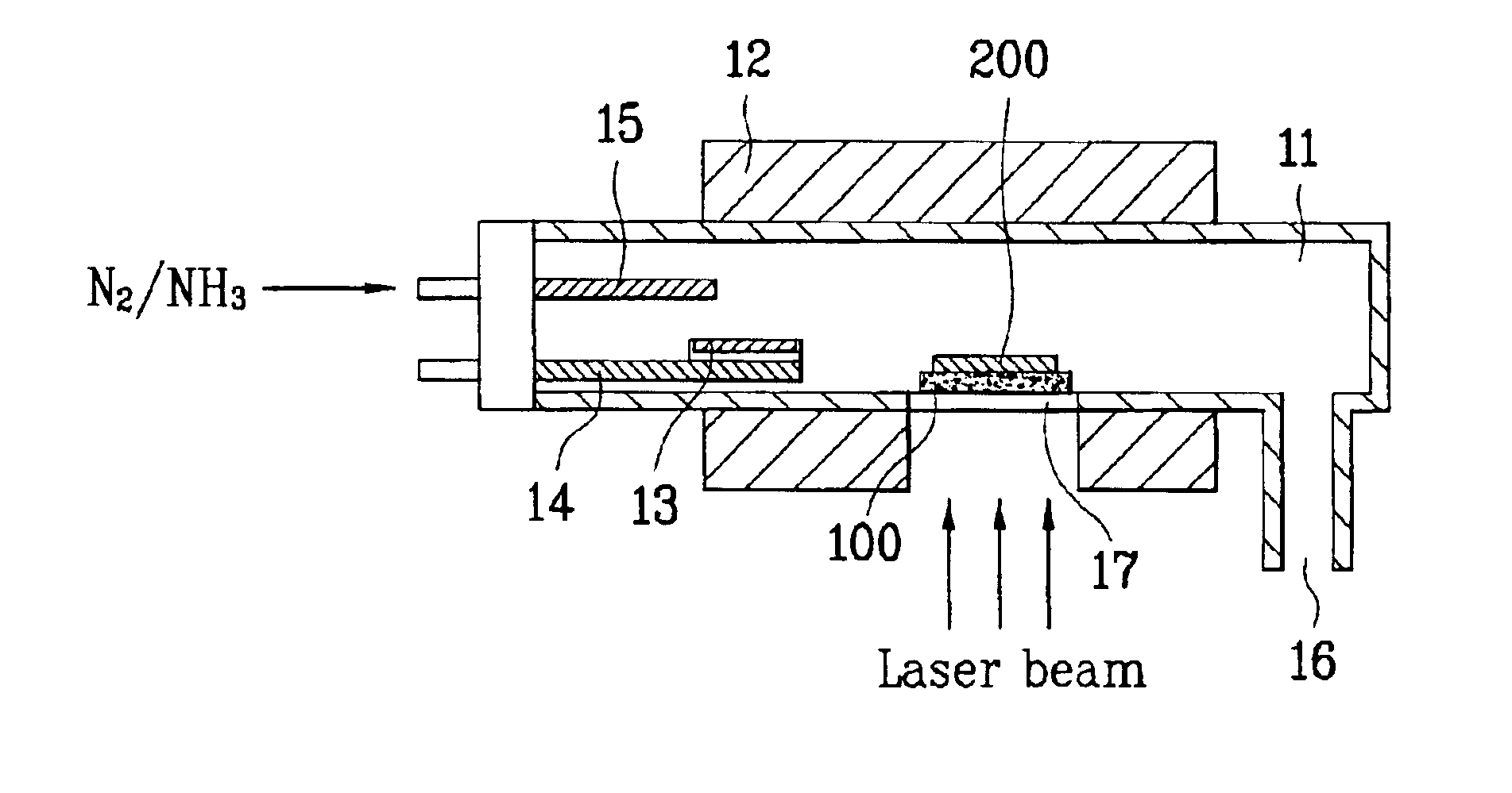
[0029]FIG. 1 illustrates a cross-sectional view of an apparatus for manufacturing a GaN substrate according to a first embodiment of the present invention.

[0030]An apparatus for manufacturing a GaN substrate according to a first embodiment of the present invention is characterized in that a substrate and a GaN layer are separated from each other by carrying out a laser lift-off process in the same chamber without transferring the substrate having the GaN layer grown thereon.

[0031]Referring to FIG. 1, an apparatus for manufacturing a GaN substrate according to a first embodiment of the present invention includes a chamber 11 for loading a substrate 100 therein, a heating means 12 installed outside the chamber 11 to heat the chamber 11 to a high temperature of at least 1,000° C., a Ga boat 14 installed inside the chamber 11 to receive a GaN powder, a Ga powder or a mixed powder 13 of GaN and Ga for sublimating Ga molecules by a heat, an injection pipe 15 injecting a gas such as N...

second embodiment

[0037

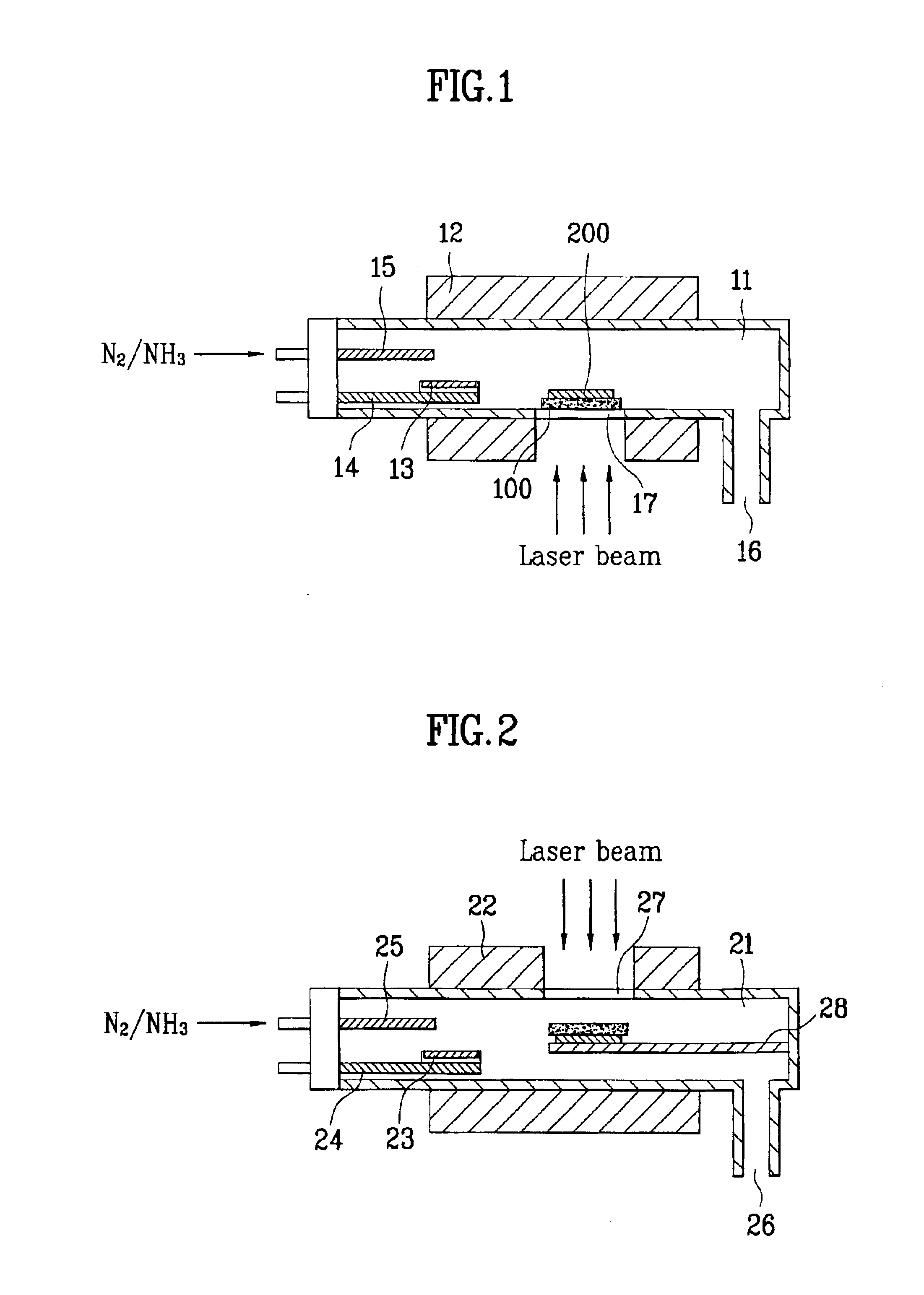
[0038]FIG. 2 illustrates a cross-sectional view of an apparatus for manufacturing a GaN substrate according to a second embodiment of the present invention.

[0039]An apparatus for manufacturing a GaN substrate according to a second embodiment of the present invention is characterized in that a GaN layer is grown on a substrate, a bottom face of the substrate is disposed to confront a transparent window, and the substrate and the GaN layer are separated from each other by carrying out a laser lift-off process in the same chamber.

[0040]Referring to FIG. 2, an apparatus for manufacturing a GaN substrate according to a second embodiment of the present invention includes a chamber 21 for loading a substrate 100 therein, a heating means 22 installed outside the chamber 21 to heat the chamber 21 to a high temperature of at least 1,000° C., a Ga boat 24 installed inside the chamber 21 to receive a GaN powder, a Ga powder or a mixed powder 23 of GaN and Ga for sublimating Ga molecules by...

third embodiment

[0047

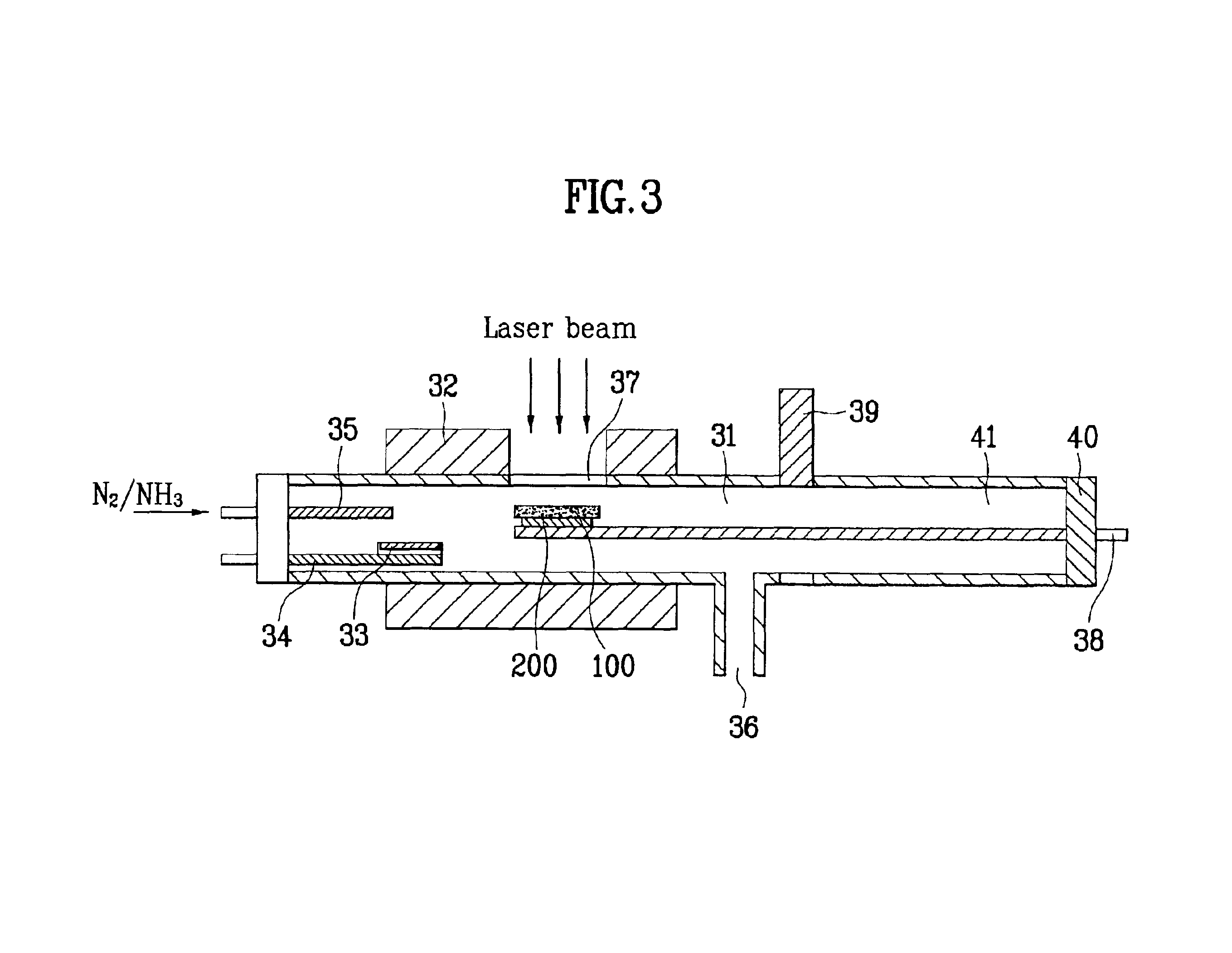
[0048]FIG. 3 illustrates a cross-sectional view of an apparatus for manufacturing a GaN substrate according to a third embodiment of the present invention.

[0049]Referring to FIG. 3, an apparatus for manufacturing a GaN substrate according to a third embodiment of the present invention includes a chamber 31 for loading a substrate 100 therein, a heating means 32 installed outside the chamber 31 to heat the chamber 31 to a high temperature of at least 1,000° C., a Ga boat 34 installed inside the chamber 21 to receive a GaN powder, a Ga powder or a mixed powder 33 of GaN and Ga for sublimating Ga molecules by a heat, an injection pipe 35 injecting a gas such as N2, NH3, or the like in the chamber 31 to grow a GaN layer 200 on the substrate 100 by having nitrogen molecules react chemically on the Ga molecules sublimated from the Ga boat 34, an exhaust pipe 36 discharging a gas in the chamber 31 externally, a transparent window 37 at an upper portion of the chamber 31 to apply a las...


PUM

PropertyMeasurementUnit
temperatureaaaaaaaaaa
wavelengthaaaaaaaaaa
transparentaaaaaaaaaa

Abstract

Disclosed are an apparatus for manufacturing GaN substrate and a manufacturing method thereof enabling to prevent micro-cracks or bending of a GaN substrate by separating a substrate and a GaN layer from each other after growing the GaN layer on the substrate in the same chamber. The present invention includes a chamber for loading a substrate therein, a heating means heating the chamber, a Ga boat installed inside the chamber to receive a Ga molecule producing material, an injection pipe injecting a nitrogen molecule producing gas in the chamber, the nitrogen molecule producing gas reacting chemically on the Ga molecule producing material to form a GaN layer on the substrate, and a transparent window at a circumference of the chamber to apply a laser beam to the substrate.

Description

[0001]This application claims the benefit of the Korean Application No. P2001-81877 filed on Dec. 20, 2001, which is hereby incorporated by reference.BACKGROUND OF THE INVENTION[0002]1. Field of the Invention[0003]The present invention relates to an apparatus for manufacturing a luminous element substrate and a manufacturing method thereof, and more particularly, to an apparatus for manufacturing GaN substrate and a manufacturing method thereof.[0004]2. Discussion of the Related Art[0005]As demands on short-wavelength luminous elements of high efficiency are increased lately, a bluish-purple short-wavelength luminous element becomes a matter of great interest. Specifically, a blue light-emitting diode has a long luminous time and is widely applicable to various fields such as multimedia, information communication, and the like. Such a blue light-emitting diode generates a short-wavelength of about 450 nm, thereby enabling to improve a processing rate of an information processing sys...

Claims


Application Information

Patent Timeline
Patent Type & Authority Patents(United States)
IPC IPC(8): C23C14/06C23C14/00C30B23/02C30B25/02H01L33/00
CPCC23C14/0005C23C14/0641C23C14/228C30B23/02C30B29/406C30B25/02Y10T117/1004Y10S117/915Y10T117/1008
Inventor KIM, CHIN KYO
Owner LG ELECTRONICS INC
Why Eureka
Try Eureka