Method and apparatus for polishing a copper layer and method for forming a wiring structure using copper

a technology of cu and wiring structure, which is applied in the direction of electrical equipment, semiconductor/solid-state device manufacturing, basic electric elements, etc., can solve the problems of cu being rapidly diffused into silicon or other metal layers, and affecting the quality of cu wiring

Inactive Publication Date: 2005-08-02
SAMSUNG ELECTRONICS CO LTD
View PDF20 Cites 6 Cited by
  • Summary
  • Abstract
  • Description
  • Claims
  • Application Information

AI Technical Summary

Benefits of technology

[0013]The present invention addresses the limitations of the conventional approaches. In this manner, a polishing system and method are provided for forming Cu wiring having improved planarization, while mitigating scratches during fabrication, and improving yield.
[0014]It is a first object of the present invention to provide a method for polishing a Cu metal layer capable of reducing process failure.
[0015]It is a second object of the present invention to provide an apparatus for polishing a Cu metal layer adapted for reducing process failure.
[0016]It is a third object of the present invention is to provide a method for forming a Cu metal wiring structure capable of reducing process failure.
[0020]In the apparatus and system of the present invention, the Cu oxide layer is removed prior to polishing, such that scratches or other failure-inducing features that would otherwise be caused by the presence of the Cu oxide layer can be mitigated or prevented.

Problems solved by technology

However, as semiconductor devices become more highly integrated, the aluminum wiring structure exhibits limitations such as a junction spike failure and electromigration.
However, Cu is rapidly diffused into silicon or other metal layers during processing.
Thus, a conventional photolithography process is not suitable for Cu wiring.
In addition, the polishing rate at each part of the silicon wafer varies depending on the corresponding thickness of the Cu oxide layer 18, so that the polishing uniformity is adversely affected.
However, it is very difficult to optimize the process condition such that the oxidation can be performed to an upper portion of the wiring, that is, to the very upper portion of the trench.

Method used


Image

  • Method and apparatus for polishing a copper layer and method for forming a wiring structure using copper
  • Method and apparatus for polishing a copper layer and method for forming a wiring structure using copper
  • Method and apparatus for polishing a copper layer and method for forming a wiring structure using copper

Examples


Embodiment Construction

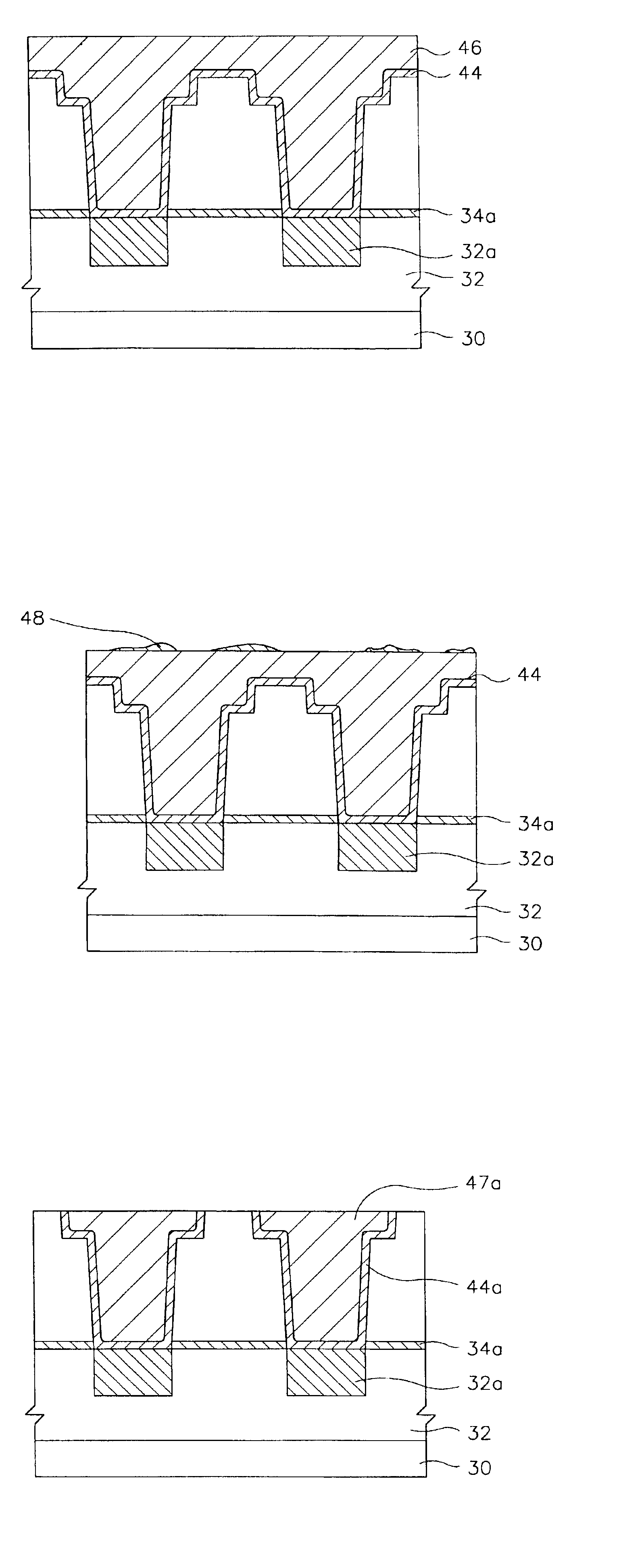
[0026]Hereinafter, a method for polishing a Cu metal layer according to one embodiment of the present invention will be described.

[0027]Initially, a silicon wafer having a Cu metal layer as an uppermost layer thereof is prepared. In order to form the Cu metal layer, a relatively thin Cu seed layer is formed, which is, in effect, a pre-treatment process for forming the Cu metal layer. The Cu seed layer is used as an electrode during a subsequent Cu plating process. Then, Cu is plated on the Cu seed layer through an electroplating process, thereby forming the Cu metal layer. By performing the electroplating process, pure Cu metal is extracted on a surface of a cathode by an electrolysis action. The Cu metal formed by the electroplating process has a metastable state, in which crystal grains are non-uniformly arranged. For this reason, the Cu metal layer is annealed (heat-treated) for crystallizing the Cu metal layer. The annealing (or heat-treating) process is carried out, for example...


PUM

PropertyMeasurementUnit
temperatureaaaaaaaaaa
thicknessaaaaaaaaaa

Abstract

In a method and apparatus for polishing a Cu metal layer and a method for forming Cu metal wiring, Cu oxide created by a surface oxidation of a Cu metal layer is removed from the wafer. The Cu metal layer, in which Cu oxide is removed, is polished. By polishing the Cu metal layer using the above method, process failures, such as scratches, caused by the presence of remnants of Cu oxide during subsequent polishing can be prevented.

Description

BACKGROUND OF THE INVENTION[0001]1. Field of the Invention[0002]The present invention relates to a method and apparatus for polishing a copper (Cu) layer and a method for forming a wiring structure using Cu, and more particularly to a method for polishing a Cu layer formed by an electro-plating and annealing process, a polishing apparatus that is suitable for performing the polishing method, and a method for forming a wiring structure using Cu.[0003]2. Description of the Related Art[0004]As information media, such as computers, continue to become more widely used, associated semiconductor technology must continue to advance. Functionally, semiconductor devices must operate at high speeds with ever-increasing storage capacity. Accordingly, semiconductor technology has evolved to continually improve the degree of integration, reliability and performance of semiconductor devices. For this reason, there are strict requirements for electric wiring techniques.[0005]In a conventional elect...

Claims


Application Information

Patent Timeline
Patent Type & Authority Patents(United States)
IPC IPC(8): H01L21/70H01L21/321H01L21/768H01L21/02H01L21/3213H01L21/304
CPCH01L21/02074H01L21/3212H01L21/32134H01L21/76838H01L21/7684H01L21/304
Inventor HAN, JA-HYUNGHAH, SANG-ROKSON, HONG-SEONGHONG, DUK-HOPARK, BYUNG-LYUL
Owner SAMSUNG ELECTRONICS CO LTD
Why Eureka
Try Eureka