Liquid-crystal display device and method of fabricating the same

a technology of liquid crystal display and display device, which is applied in the direction of instruments, polarising elements, lenses, etc., can solve the problems of narrow viewing angle, improvement of fast response of lcd device, and high probability of problem, so as to improve the fast response characteristics

Inactive Publication Date: 2005-08-02
NEC LCD TECH CORP
View PDF21 Cites 48 Cited by
  • Summary
  • Abstract
  • Description
  • Claims
  • Application Information

AI Technical Summary

Benefits of technology

[0021]Accordingly, a chief object of the present invention is to provide a LCD device that improves the fast response characteristics, and a method of fabricating the device.
[0022]Another object of the present invention is to provide a LCD device that improves not only the viewing characteristics but also the fast response characteristics, and a method of fabricating the device.
[0023]Still another object of the present invention is to provide a LCD device that makes it possible to decrease effectively the necessary accuracy in placement and / or alignment of constituent elements or parts, and a method of fabricating the device.

Problems solved by technology

However, due to the peculiar actions to the liquid crystal molecules under application of the voltage, there is a problem that the obtainable viewing angle is narrow.
However, there are still many problems on improvement of fast response of LCD devices.
Thus, a problem is likely to occur.
In particular, if the LCD panel is large-sized, a problem of signal transmission delay along the wiring lines and / or insufficient writing voltage to the TFTs will occur.
In this case, however, there arises a problem that the viewing angle is narrowed due to the birefringence of liquid crystal.
As a result, there arises a problem that the light is transmitted even in the black displaying state or the contrast degrades.
Furthermore, if the product (Δn·d) of the optical anisotropy Δn and the cell thickness d is increased, there arises a problem that the viewing angle is narrowed.
This causes a problem that the fabrication yield of the LCD panel degrades.
Moreover, another problem that luminance decreases in part of the pixel occurs.

Method used


Image

  • Liquid-crystal display device and method of fabricating the same
  • Liquid-crystal display device and method of fabricating the same
  • Liquid-crystal display device and method of fabricating the same

Examples


first embodiment

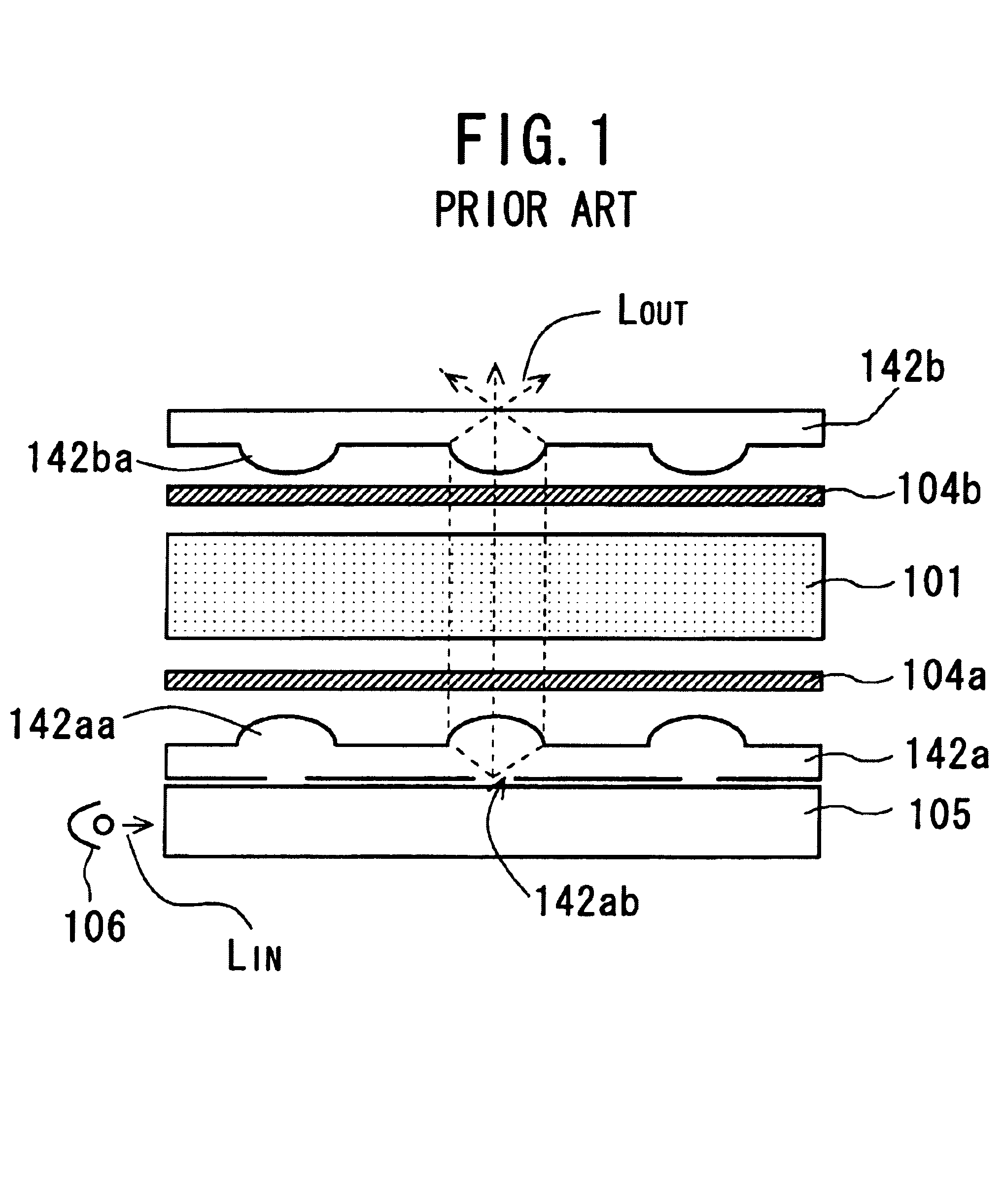
[0156]FIG. 2 shows the structure of a LCD device according to a first embodiment of the invention. FIGS. 3A and 3B and 4A to 4D show the operation principle of the device, respectively.

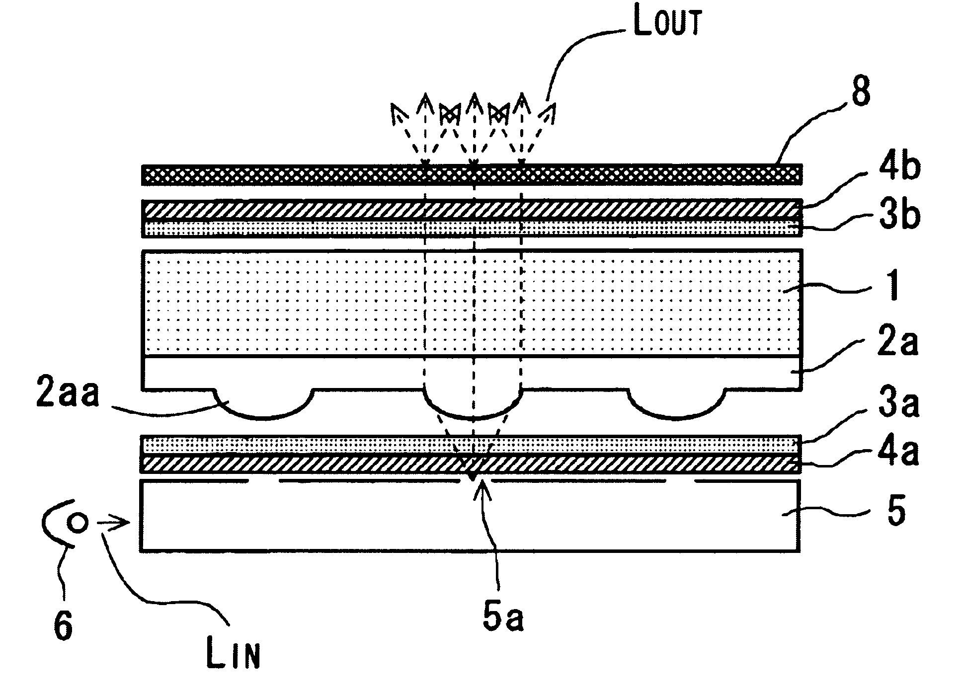
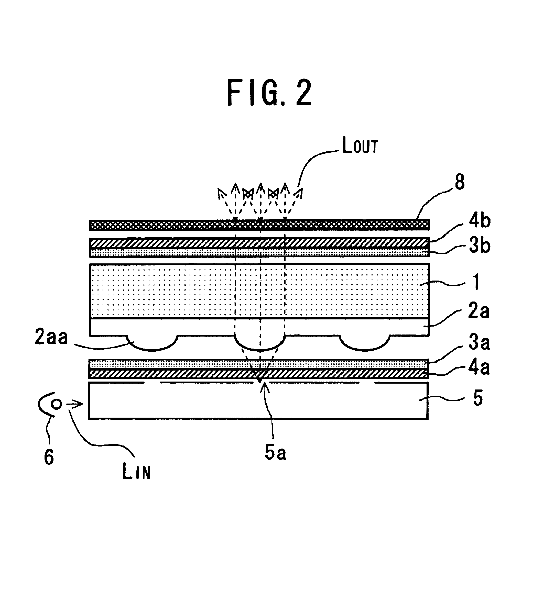
[0157]The LCD device of FIG. 2 comprises a liquid crystal section or cell 1 having a first substrate, a second substrate, and a liquid crystal layer. The first and second substrates are fixed in parallel to each other while the liquid crystal layer is interposed between these two substrates. Switching elements such as TFTs are formed on the first substrate. Thus, the first substrate may be termed the “TFT substrate”, and the second substrate may be termed the “counter or opposite substrate”.

[0158]The LCD device further comprises a microlens array 2a, quarter wavelength (λ / 4) plates 3a and 3b, polarizer plates 4a and 4b, a light guide plate 5, a light source 6, and a viewing-angle controller plate 8. The microlens array 2a, the quarter wavelength plate 3a, the polarizer plate 4a, the guide plate 5, and...

second embodiment

[0188]FIG. 5 shows the structure of a LCD device according to a second embodiment of the invention. This device has the same configuration as the device of the first embodiment, except that the microlens array 2a is united with the guides plate 5, not the section 1.

[0189]The LCD device of FIG. 5 comprises a liquid crystal section 1 having a first substrate (a TFT substrate), a second substrate (a counter or opposite substrate), and a liquid crystal layer. The first and second substrates are fixed in parallel to each other while the liquid crystal layer is interposed between these two substrates. Switching elements such as TFTs are formed on the first substrate.

[0190]The LCD device of FIG. 5 further comprises a microlens array 2b, quarter wavelength (λ / 4) plates 3a and 3b, polarizer plates 4a and 4b, a light guide plate 5, a light source 6, and a viewing-angle controller plate 8. The microlens array 2b, the quarter wavelength plate 3a, the polarizer plate 4a, the guide plate 5, and t...

third embodiment

[0200]The third embodiment of the invention relates to a method of fabricating a LCD device. FIGS. 6A to 6C show the process steps of the method and FIG. 7 shows the configuration of a laser apparatus used therefor.

[0201]In the following explanation, the TFT substrate 10 on which TFTs are formed is fabricated in a known, ordinary method and therefore, only the process steps of forming the microlens array are explained.

[0202]First, as shown in FIG. 6A, a polycarbonate sheet or plate 11 with a thickness of approximately 50 μm is attached on the back of the TFT substrate 10 with or without an adhesive.

[0203]Next, as shown in FIG. 6B, for example, KrF excimer laser light 13 with a wavelength of 248 nm is irradiated to the sheet 11 in the form of pulse. The irradiation is carried out at approximately 500 pulses while the light 13 is aligned with respect to the substrate 10 using the metal wiring lines, semiconductor layers, and / or alignment marks on the substrate 10.

[0204]The energy inte...


PUM

PropertyMeasurementUnit
thicknessaaaaaaaaaa
thicknessaaaaaaaaaa
angleaaaaaaaaaa

Abstract

A LCD device is provided. On the input side, the collimated-light generator generates collimated light from incident light and then, the first polarizer plate of the first polarized-light controller generates first polarized light from the collimated light. The first quarter wavelength plate of the first polarized-light controller generates second polarized light from the first polarized light. The second polarized light thus generated passes through the liquid crystal layer to reach the output side. On the output side, the second polarized light passes through the second quarter wavelength plate of the second polarized-light controller and the second quarter wavelength plate thereof. Thus, the polarization state of the second polarized light is returned to its original one.

Description

BACKGROUND OF THE INVENTION[0001]1. Field of the Invention[0002]The present invention relates generally to Liquid-Crystal Display (LCD) device. More particularly, the invention relates to a LCD device that makes it possible to achieve wide viewing angle and fast response, and a method of fabricating the device.[0003]2. Description of the Related Art[0004]Conventionally, LCD devices have been extensively used for electronic equipment designed for so-called Office Automation (OA) and portable communication and / or information-management terminals. This is because LCD devices have the advantage of compact, thin, and low power consumption.[0005]With LCD devices, the alignment or orientation of liquid crystal molecules is changed by a voltage applied across the liquid crystal layer to thereby control the penetration of light utilizing a variety of the optical properties of the liquid crystal cell, such as the birefringence effect and rotary polarization. LCD devices are classified into va...

Claims


Application Information

Patent Timeline
Patent Type & Authority Patents(United States)
IPC IPC(8): G02F1/13G02F1/1335G02F1/139G02B1/04G02B3/00G02B5/20G02B5/02G02B5/30G02F1/1334G02F1/13363
CPCG02F1/133526G02F1/1393G02F2001/133638G02F1/133638G02F1/1335
Inventor OKUMURA, HIROSHISUZUKI, MASAYOSHI
Owner NEC LCD TECH CORP
Why Eureka
Try Eureka