Chemical filter arrangement for a semiconductor manufacturing apparatus

a manufacturing apparatus and chemical filter technology, applied in the direction of heating types, printers, separation processes, etc., can solve the problems of affecting the operation of the equipment, so as to facilitate maintenance and avoid turbulence flow on the filter surface. , the effect of reducing the space required for the apparatus

Inactive Publication Date: 2005-08-02
CANON KK
View PDF18 Cites 11 Cited by
  • Summary
  • Abstract
  • Description
  • Claims
  • Application Information

AI Technical Summary

Benefits of technology

[0019]With the arrangement described above, turbulence flows on the filter surface can be avoided or reduced. Also, the space required for the apparatus is reduced, and easiness of maintenance is facilitated. As a result, the performance of the apparatus can be held for a long term, and effective utilization of the clean room is assured.

Problems solved by technology

Therefore, recently, they are used prevalently as a resist for excimer laser light with which illuminance is not easily obtainable.
This causes deterioration of image profile.
With the shortening of exposure wavelength, there arises a problem of blurring of optical components irradiated with exposure light, causing a decrease of exposure amount on the wafer surface.
This results in enlargement of the required filter space which causes an increase in size of the apparatus.
As a result, a large filter area is required.
Also, for replacement of chemical filters, since it should be done at the ceiling of the apparatus chamber, the replacement work is dangerous and poor in efficiency.
However, anyway, this leads to bulkiness of the apparatus.
On the other hand, in chemical filters, non-uniformess of flow velocity easily occurs in the same plane, causing variation in lifetime and, as a result, degradation of apparatus performance.

Method used


Image

  • Chemical filter arrangement for a semiconductor manufacturing apparatus
  • Chemical filter arrangement for a semiconductor manufacturing apparatus
  • Chemical filter arrangement for a semiconductor manufacturing apparatus

Examples


Embodiment Construction

[0025]Preferred embodiments of the present invention will now be described with reference to the attached drawings.

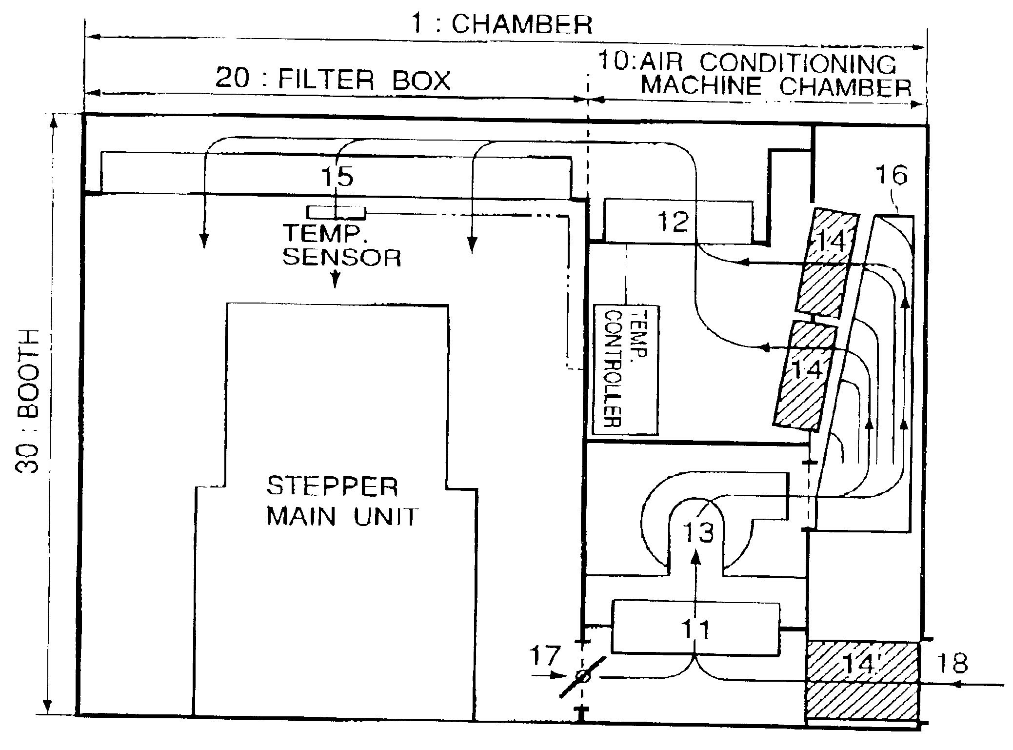
[0026]FIG. 1 shows a general structure of an exposure apparatus. For the gas (air) conditioning of a main unit of this exposure apparatus, there is a chamber 1. This chamber 1 includes an air conditioning machine room 10 mainly for performing temperature control of the air, a filter box 20 for filtering small foreign particles to provide a uniform flow of clean airs, and a booth 30 for intercepting the apparatus environment from the outside.

[0027]In this chamber 1, an air which is temperature controlled by a cooling device 11 and a re-heater 12, disposed inside the air conditioning machine room 10, is supplied into the booth 30 by means of a blower 13 and through a chemical filter 14 and a dust removing filter 15. The air supplied into the booth 13 is caught by a return port 17 and, again, it is taken back to the air conditioning machine room 10 and thus circulated in t...


PUM

PropertyMeasurementUnit
flow velocityaaaaaaaaaa
pressure lossaaaaaaaaaa
air flow velocityaaaaaaaaaa

Abstract

Disclosed is a semiconductor exposure apparatus which includes a chamber for accommodating therein a main unit of the exposure apparatus, a gas controlling unit for controlling a gas in the chamber, a chemical filter for attracting a chemical substance in a controlling gas, and a dust removing filter for catching a dust particle in a controlling gas, wherein a gas blowing area of the chemical filter is smaller than that of the dust removing filter, wherein said chemical filter and said dust removing filter are disposed separately from each other. The chemical filter is mounted obliquely with respect to a direction of flow of a supplied gas. A gas rectifying device is disposed at a gas inlet side of the chemical filter and the dust removing filter. The chemical filter can be a pleat filter, and it is mounted so that the pleat thereof is orthogonal to the direction of flow of the supplied air.

Description

FIELD OF THE INVENTION AND RELATED ART[0001]This invention relates to a semiconductor manufacturing system suitably usable in production of semiconductor devices, particularly, in a semiconductor exposure apparatus.[0002]The manufacture of IC, LSI or liquid crystal panel include many processes to be executed for a substrate such as a semiconductor wafer substrate or a glass substrate. An exposure process (pattern printing process) among them is a very important process, being a pivot of the semiconductor manufacture. Exposure apparatuses such as stepper or scanner are known as an apparatus for performing this process.[0003]As a resist material to be applied to a wafer, generally, there are high molecular films in which chemical reaction can be produced efficiently in response to irradiation with ionizing radiation, and chemical amplification resists in which a catalyst (acid) is produced by exposure and, through a baking process (PEB), image formation is carried out on the basis of ...

Claims


Application Information

Patent Timeline
Patent Type & Authority Patents(United States)
IPC IPC(8): B01D46/10B01D53/04F24F3/16G03F7/20B01D46/00B01D46/52H01L21/02H01L21/027
CPCB01D46/0036B01D46/12B01D46/521B01D53/0446F24F3/161G03F7/70858G03F7/70916B01D53/0438B01D53/0454B01D2253/102B01D2253/206B01D2253/3425B01D2257/30B01D2257/70B01D2258/0216B01D2267/40F24F2003/1621F24F8/15F24F3/167
Inventor NAKANO, HITOSHIARAKAWA, KIYOSHI
Owner CANON KK
Why Eureka
Try Eureka