
Power semiconductor device having semiconductor-layer-forming position controlled by ion implantation without using photoresist pattern, and method of manufacturing such power semiconductor device

a technology of power semiconductor and ion implantation, which is applied in the direction of semiconductor devices, basic electric elements, electrical appliances, etc., can solve the problems of avalanche breakdown and decrease the breakdown voltage, and achieve the effect of preventing a decrease in the breakdown voltage and reducing the photolithography process steps

Inactive Publication Date: 2005-08-09
MITSUBISHI ELECTRIC CORP
View PDF5 Cites 32 Cited by
  • Summary
  • Abstract
  • Description
  • Claims
  • Application Information

AI Technical Summary

Benefits of technology

[0018]An object of the present invention is to provide a power semiconductor device capable of reducing photolithography process steps and preventing a decrease in breakdown voltage due to the reduction of the process steps, and to provide a method of manufacturing such a power semiconductor device.
[0021]The present invention allows reduction of photolithography process steps and can prevent a decrease in breakdown voltage due to the reduction of the process steps.

Problems solved by technology

If the strength of an electric field applied to the depletion layer exceeds a certain value with increased voltage, an avalanche breakdown occurs.
If the photolithography process step that is used in forming the n+ source layer is eliminated for reduction of manufacturing process steps, the following problem arises.
This can easily cause punch-through, thereby decreasing the breakdown voltage.

Method used


Image

  • Power semiconductor device having semiconductor-layer-forming position controlled by ion implantation without using photoresist pattern, and method of manufacturing such power semiconductor device
  • Power semiconductor device having semiconductor-layer-forming position controlled by ion implantation without using photoresist pattern, and method of manufacturing such power semiconductor device
  • Power semiconductor device having semiconductor-layer-forming position controlled by ion implantation without using photoresist pattern, and method of manufacturing such power semiconductor device

Examples


Embodiment Construction

[0109]First Preferred Embodiment

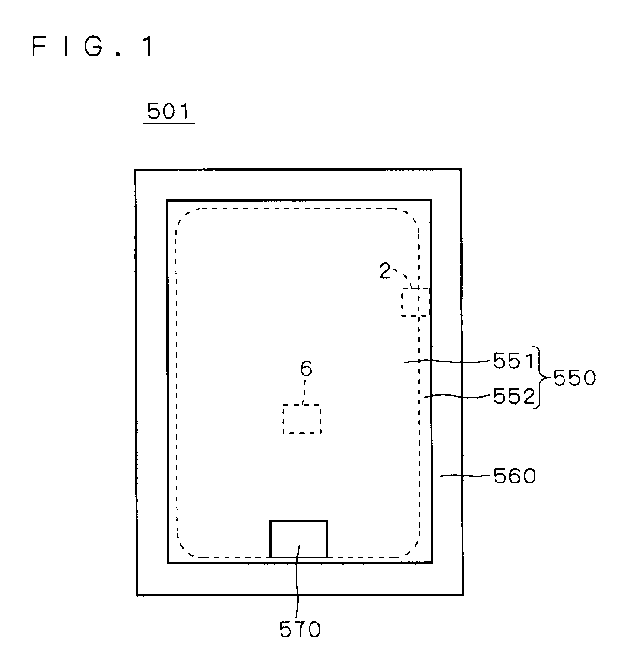
[0110]FIG. 1 shows a plan view for explaining a power semiconductor device (hereinafter also referred to simply as a “semiconductor device”) 501 according to a first preferred embodiment.

[0111]As shown in FIG. 1, the semiconductor device 501 is roughly divided into an element configuration part 550 and a dicing part 560 surrounding the element configuration part 550. The element configuration part 550 includes a central region (or cell region) 551 and an outer peripheral region 552 surrounding the central region 551.

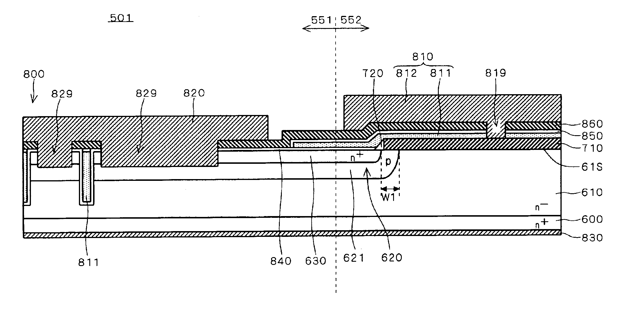
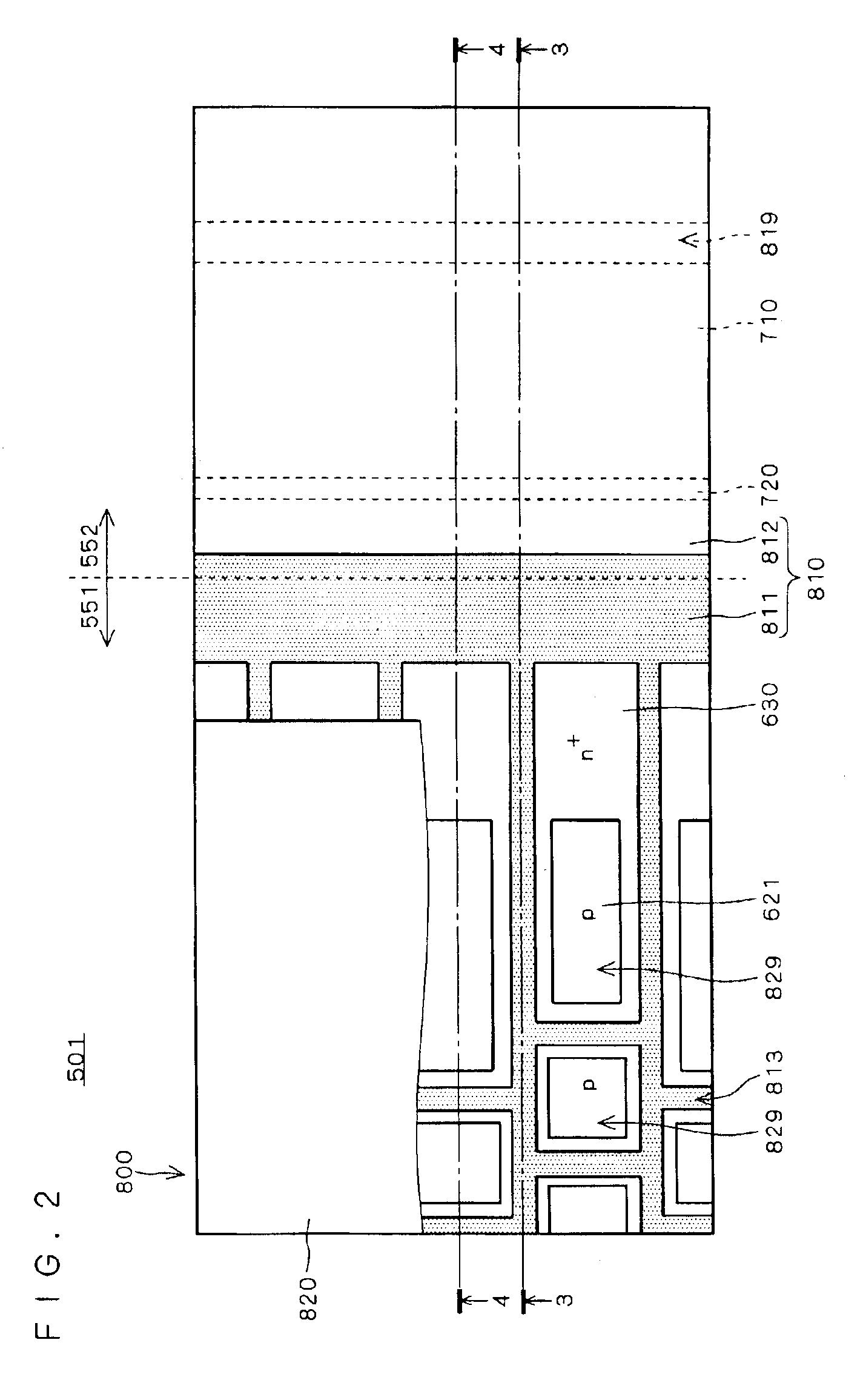
[0112]FIG. 2 shows an enlarged plan view of a portion 2 encircled by dashed line in FIG. 1 (a portion in the vicinity of the boundary between the central region 551 and the outer peripheral region 552). FIG. 3 shows a cross-sectional view (of a silicon mesa region) taken along line 3—3 of FIG. 2, FIG. 4 shows a cross-sectional view taken along line 4—4 of FIG. 2, and FIG. 5 shows part of FIG. 3 (or FIG. 4) in enlarged dimension. FIG. 6 sho...


PUM


Abstract

A first insulator (710) having an opening within a central region (551) is formed on a main surface (61S) of an epitaxial layer (610). Then, p-type impurities are ion implanted through the opening of the first insulator (710) and then heat treatment is carried out, thereby to form a p base layer (621) in the main surface (61S). An insulating film is formed to fill in the opening and then etched back, thereby to form a second insulator (720) on a side surface (71W) of the first insulator (710). Under conditions where the second insulator (720) is present, n-type impurities are ion implanted through the opening and then heat treatment is carried out, thereby to form an n+ source layer (630) in the main surface (61S) of the p base layer (621).

Description

BACKGROUND OF THE INVENTION[0001]1. Field of the Invention[0002]The present invention relates to a power semiconductor device and a method of manufacturing the same, and especially to a technique for reducing photolithography process steps and preventing a decrease in breakdown voltage due to the reduction of the process steps.[0003]2. Description of the Background Art[0004]A conventional power MOSFET (Metal Oxide Semiconductor Field Effect Transistor) is manufactured as follows.[0005]First, an n−-type silicon layer is grown epitaxially on an n+-type silicon substrate. A silicon oxide film (hereinafter also referred to as an “oxide film”) is then formed on a main surface of the above epitaxial layer. A photoresist pattern is formed on the oxide film using photolithography techniques and using the photoresist pattern as a mask, a portion of the oxide film which is located within a central region of an element configuration part is etched to form an opening. At this time, a portion of...

Claims


Application Information

Patent Timeline
IPC IPC(8): H01L21/02H01L21/331H01L21/336H01L29/08H01L29/10H01L29/423H01L29/02H01L29/40H01L29/06H01L29/739H01L29/78
CPCH01L29/7813H01L29/7397H01L29/66348H01L29/1095H01L29/4238H01L29/7811H01L29/78
Inventor NARAZAKI, ATSUSHI
Owner MITSUBISHI ELECTRIC CORP
Learn More